ASIA ELECTRONICS INDUSTRYYOUR WINDOW TO SMART MANUFACTURING
SEM Delivers High-Resolution Mask Line Measurement
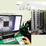
Masks or reticles transfer circuit patterns onto wafers. Critical dimension scanning electron microscopes (CD-SEMs) made by HOLON CO., LTD. measure the sizes of the original versions of the mask. These microscopes are used by mask manufacturers to measure line width.
Unlike those for research, SEMs used in production facilities need to measure objects at high speeds in a non-destructive manner. A SEM emits a beam of electrons in a vacuum in order to prevent them from colliding with molecules. The sample is placed in a vacuum chamber. Each time the chamber is opened and closed, it becomes open to the atmosphere and thus needs to be returned to a vacuum state. A SEM used for production facilities, meanwhile, automatically takes in and discharges the sample to maintain a vacuum state.
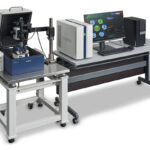
High-Resolution Electron Microscope
Manufactured masks are accompanied by length measurement data before they are delivered to a semiconductor plant. Lithography parameters are set based on the data.
The surfaces of wafers are exposed to laser light through masks so that mask patterns are transferred with their sizes reduced to one fourth. This is called an exposure process.
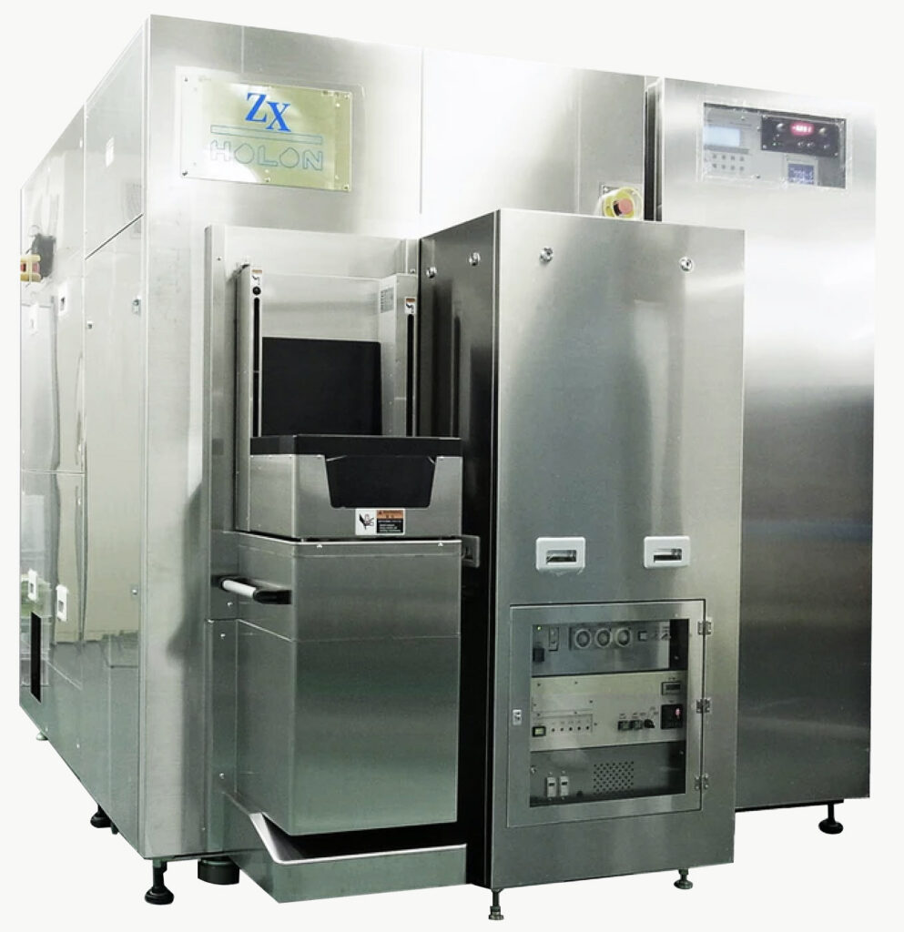
Electron microscopes can cause a blur if there is an aberration during image formation (blur during imaging). HOLON’s ZX CD-SEM offers high resolution (1.5nm) by removing as many aberrations as possible using its improved column (lens tube) through which a beam of electrons passes. Since its launch in 2017, ZX has been delivered to factories for the latest products.
Offers Good Detectability
Meanwhile, the LEXa-10 machine, which evaluates defects, also uses a beam of electrons. It detects particles of unnecessary elements on the surfaces of masks. It adjusts the probe current (current in the probe that is emitted to the sample) when emitting a beam of electrons to reduce damage to the sample.
The beam acceleration voltage of conventional SEMs is 10 to 15kV, while that of LEXa-10 is reduced to 7kV or less.
Hao Zhang, President and Chief Executive Officer of HOLON, says “Heavy elements become difficult to detect if the acceleration voltage is too low.” While the minimum acceleration voltage of LEXa-10 is 0.5kV, it can minimize damage to the sample during measurement while offering good detectability.
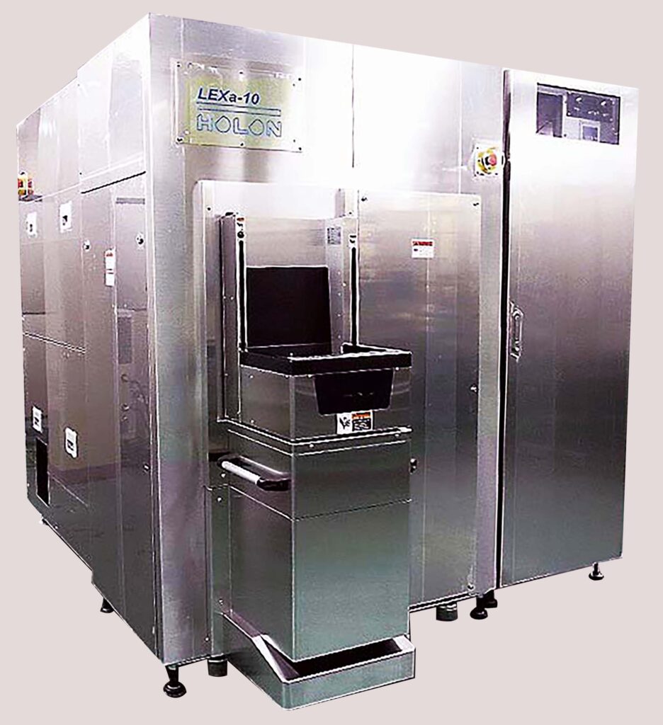
When observing a defect in a mask, it first records the coordinates of the location of the defect. Then, it carries out analysis based on the coordinates. It identifies unnecessary elements by comparing the X-ray spectrum with the spectrum on the database. This makes it possible to find out in which manufacturing process and why particles were produced on the surfaces of masks.
Eyes Next-Generation SEM
As demand rapidly increased for semiconductor inspection and measurement, HOLON relocated its headquarters to Tachikawa City in Tokyo in July 2021. It now has a cleanroom three times larger than the previous one. It has increased its production capacity to 20 units per year, twice larger than the previous capacity.
The company will focus efforts on developing a next-generation SEM in collaboration with its parent company A&D Company, Limited. At present, the company is developing a next-generation machine aimed for release at the end of 2022.
- Share: