ASIA ELECTRONICS INDUSTRYYOUR WINDOW TO SMART MANUFACTURING
Samsung Electro-Mechanics Unveils Advanced Chip Package Technology
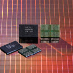
Samsung Electro-Mechanics unveiled advanced semiconductor package technology in KPCA Show 2022. It exhibited high-performance, high-integration, and ultra-slim next-generation semiconductor package substrates.
The KPCA Show (International Electronic Circuits and Packaging Show), Korea’s largest circuit board exhibition, brings together substrate, material, and equipment manufacturers from home and abroad. It was held from Sept. 21 to 23 at Songdo Convensia, Incheon.
In particular, semiconductor package substrate connects highly integrated semiconductor chip and mainboard to transmit electrical signals and power. Substrates for high-performance semiconductors used for 5G, artificial intelligence (AI), and automobiles require advanced techniques. They can increase the number of layers, implement microcircuits, achieve granular inter-layer consistency, and make products thinner to reduce the set thickness.
Flip-chip Ball Grid Array
One of the highlights is high-performance Flip-chip Ball Grid Array (FCBGA) including FCBGA for servers.
In FCBGA, the semiconductor chip and package substrate are connected in a flip chip method. Specifically, it is a highly integrated package substrate with improved electrical and thermal properties. The high-spec product is mostly used for central processing units (CPU) and graphics processing units (GPU) that exchange a lot of electrical signals. Among them, FCBGA for dual servers is known to require the most complex technology.
The FCBGA for servers is a particularly complex product. It measures about 75×75mm in size (area), four times that of general FCBGA. Additionally, it has 20 or more internal layers, twice that of general products, and is designed to process high-speed signals. The product will be in production by the end of the year.
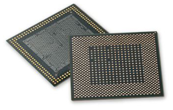
Flip Chip Chip Scale Package
Samsung Electro-Mechanics also showcased ultra-small high-density semiconductor substrates for mobile IT devices. Flip Chip Chip Scale Package (FCCSP) is a product that reduced the thickness by 50 percent compared to existing products. It has a coreless method that removes the core (inner support layer) inside the semiconductor substrate. Meanwhile, System in Package (SiP) in which several semiconductor chips and passive components such as MLCC are embedded in a package substrate, was also on display.
Chang Duckhyun, CEO of Samsung Electro-Mechanics, said, “The next-generation package substrate will become a platform that integrates all systems.”
System on Substrate
Meanwhile, System on Substrate (SoS) is a package substrate using an ultra-miniaturization process. It implements an integrated system by arranging two or more semiconductor chips on a substrate. In general, System on Chip (SoC) refers to the integration of semiconductors such as CPU and GPU into one chip. However, it involves difficulties such as limitations in implementing miniaturization of different semiconductors and utilization of space.
SoS is a next-generation substrate technology that improves semiconductor performance by placing different semiconductor chips on a single substrate and connecting them with a fine rewiring technique.
Samsung Electro-Mechanics, which started its circuit board business in 1991, has become an industry leader that supplies products to global companies with differentiated technology. In semiconductor package substrates for high-end mobile APs, it has maintained its unrivaled leadership in terms of market share and technology.
It has been intensively developing semiconductor package substrates. In general, it has made a cumulative investment of 1.9 trillion won since the end of last year, in a proactive effort to maintain the “super-gap” technology. Samsung Electro-Mechanics is focusing on fostering the semiconductor package substrate business. It has been strengthening its competitiveness based on its original manufacturing technology, dedicated facilities, and core technologies to build ultra-slim, large-area, multi-layered, parts-integrated, and microcircuit products.
- Share: