ASIA ELECTRONICS INDUSTRYYOUR WINDOW TO SMART MANUFACTURING
AFM Makes Optimal 3D Measurement with SEM
As the roughness of the silicon wafer affects the formation of fine patterns, the surface of the thin film is required to have a high degree of flatness. For state-of-the-art products, the roughness needs to be controlled down to 0.1nm or less.
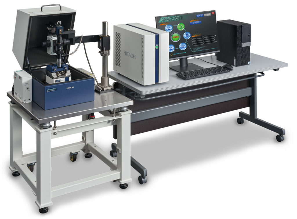
The AFM100 Series atomic force microscope (AFM) by Hitachi High-Tech Corporation can perform three-dimensional measurement. These parameters relate to observation of an object and evaluation of physical properties in the nanometer scale. A probe for scanning the sample surface on a cantilever is used. High resolution evaluation is possible in the in-plane and out-of-plane directions.
Measures Various Parameters
AFM is used for roughness evaluation after film formation and etching and for measurement of the resist pattern in semiconductor manufacturing process. Measurement using AFM is particularly required for delicate samples changing size because of damage due to electron beam irradiation. It is also used for roughness and defect observation of compound semiconductors such as silicon carbide (SiC) and gallium nitride (GaN).
AFM is increasingly demanded as an observation device and for performing measurement for different parameters corresponding to various conditions. Operating it does not require special skills and experiences. A conventional AFM is a difficult device to use, but with the new product, anybody can easily get accurate results, according to the company.
Improved Features from Electron Microscope
Unlike an electron microscope, the AFM100 Series is characterized by controlling the force acting between the probe and the sample. The motion amplitude is automatically adjusted to reduce the wear of the probe, and parameters describing vibration, deflection, and others are also optimized.
A high-resolution probe traces the sample surface to evaluate roughness, and therefore easily becomes dirty and wears frequently. The cantilever is replaced by a new one after 10 to 20 uses.
The width of the lever is about 1mm and the protrusion at the tip is only a few nanometers. Dropping the lever is possible if the user is not accustomed to handling it. Also, fine adjustment of its mounting position is not easy. The new product can be attached in a single touch using a magnet. The laser can be easily adjusted, shortening time for replacement.
Nano-level observations are performed at very high magnification. Therefore, if the heat generated by the device causes thermal expansion and the sample moves or drifts, precise observation becomes impossible. The electronic circuit, which becomes a source of heat, is placed outside the device to minimize the cause of thermal expansion. In-plane drift has been reduced to below 0.03nm per second.
Another improvement is the adoption of a low coherence laser diode called superluminescent diode (SLD). By increasing the laser output more than 10 times compared to the conventional model, significant noise reduction has been achieved.
Elemental analysis is possible with a scanning electron microscope (SEM) in contrast to AFM’s ability in height measurement. In the original Scanning Atomic and Electron Microscopy (SAEMic) correlated imaging technique, both devices are utilized together.
A special diamond-coated cantilever is used to mark the range of the sample measured by the AFM. SEM can take over the measurement smoothly for cross-check. According to Hitachi High-Tech, combining the tools can provide optimal benefit when determining the relationship between surface potential difference and electrical characteristics. The company proposes its use in defect analysis of specific parts of static SRAM.
- Share: