ASIA ELECTRONICS INDUSTRYYOUR WINDOW TO SMART MANUFACTURING
New Technologies Drive Canon’s Lithography System
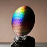
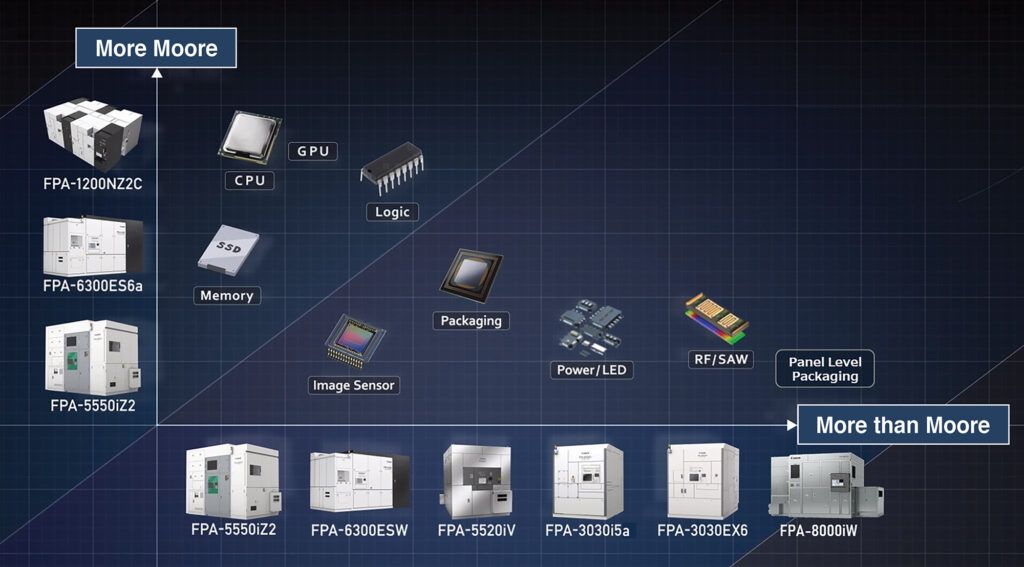
Canon Inc. deploys an extensive lineup of semiconductor lithography systems that meet diverse needs. These include systems for memories, logics, image sensors, and power devices. Also, add to these are systems for internet of things (IoT)-related devices that adopt small special substrates.
The company has also been improving productivity and overlay accuracy of i-line steppers and KrF scanners. Furthermore, it will also meet customer needs that have recently been becoming diversified.
The company’s i-line steppers and KrF scanners will continue to grow in the coming years. From here on, Canon will further improve performance and accuracy of KrF scanners. Simultaneously, the company will also strengthen proposals of solutions, and actively promote the use of i-line steppers for applications in the back-end process.
Grade Options Meet Customers’ Needs
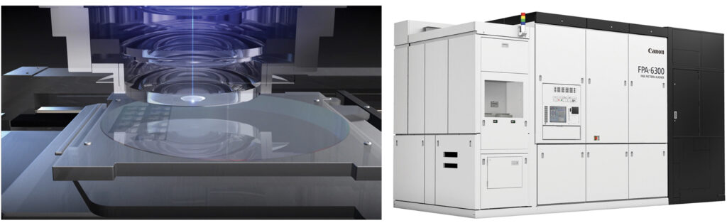
Canon has improved the productivity of the FPA-6300ES6a KrF scanner since its release in 2012. Particularly, the company has increased the exposure stage speed, optimized the wafer transfer system driving, and improved alignment sequence. Hence, reducing the exposure processing time.
The initial KrF scanner had a throughput of 200 wafers per hour (WPH). A new Grade 10 productivity upgrade option released in June 2022 for the FPA-6300ES6a has achieved 300WPH. This is the industry’s highest level of productivity for KrF scanners for 300mm wafers.
Proprietary Linear Motor Achieves Highest Acceleration
The FPA-6300ES6a’s reticle stage is fitted with Canon’s proprietary high-efficiency linear motor, which has achieved both high thrust force and high cooling efficiency. The linear motor enables the stage’s acceleration to reach 14G or higher. As it reaches the predetermined scanning speed from the resting state in a very short time, the scanner achieves significant improvement in throughput compared with its predecessor.
Achieves Both High Productivity, Overlay Accuracy
The optional high overlay (HOVL1) achieves an industry-leading overlay accuracy of 7nm (or matched machine overlay) without sacrificing throughput. In addition, it comes with Shot-Shape High Order Compensation (SSHOC), a function to change lens magnification during scanning exposure, along with the 2D-Map stage grid correction function, the KrF scanner can align the “reticle” with respect to the grid and shape of the shot of “the substrate” with higher degree of freedom. Furthermore, the adoption of a high-precision area sensor for the alignment scope has enabled alignment using arbitrary marks other than Canon’s designated marks. Thus, the scanner has significantly improved customers’ usability.
Provision of Solutions Meet Customers’ Needs
Generally, all sorts of devices need semiconductors. Hence, the demand for legacy semiconductors has also been increasing. FPA-6300ES6a supports 200mm wafers as well, and as with 300mm models, upgrade options are provided for 200mm models. Canon also provides solution programs to improve operation rate and yield, and to optimize process, thereby supporting customers that are producing diversifying devices.
Supports Wide Exposure Field
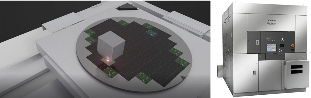
The FPA-5520iV LF i-line stepper inherits basic performance of the FPA-5520iV and is capable of single-shot exposure with a large field of 52×68mm. This is more than four times the standard exposure field (26×33mm) of front-end process lithography systems. Featuring the wide exposure field, the i-line stepper supports the manufacture of a wide range of advanced packages, including packages for the cutting-edge artificial intelligence (AI) chips, and heterogeneous packages that combine multiple large semiconductor chips. Furthermore, it also supports even larger package sizes that are expected to emerge in the future.
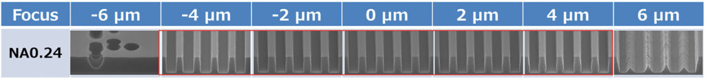
Equipped with a projection optical system with numerical aperture of 0.24 (NA0.24), the i-line stepper realizes high resolution of 1.0μm (when option is applied). Because it supports higher density package wiring accompanying the trend toward higher performance of chips, it suits the manufacture of most advanced packages. In addition, by making NA variable, it can optimize the balance between the depth of focus and resolution for line width ranging from submicron to several tens of microns.
Inherits Basic Performance of FPA-5520iV
The FPA-5520iV LF inherits basic performance and functional option of FPA-5520iV to tackle issues occurring during mass production of advanced packages. For the transfer of warped substrates, it applies the wafer transfer system, which adopts a flexible pad with an adsorption face that changes its shape in accordance with shapes of warpage of substrates. To cope with chip array variations, it comes equipped with an alignment scope with a wide field, about twice that of the conventional model.
- Share: