ASIA ELECTRONICS INDUSTRYYOUR WINDOW TO SMART MANUFACTURING
New Technology by Tokyo Electron to Enable Ultra-Fast Etching
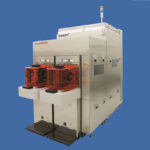
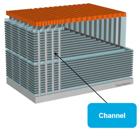
Tokyo Electron Limited announced a breakthrough development of an innovative etch technology by its team at Tokyo Electron Miyagi. Specifically, the innovative technology is capable of producing memory channel holes in advanced 3D NAND devices with a stack of over 400 layers. Tokyo Electron Miyagi is the development and manufacturing site for Tokyo Electron’s plasma etch system.
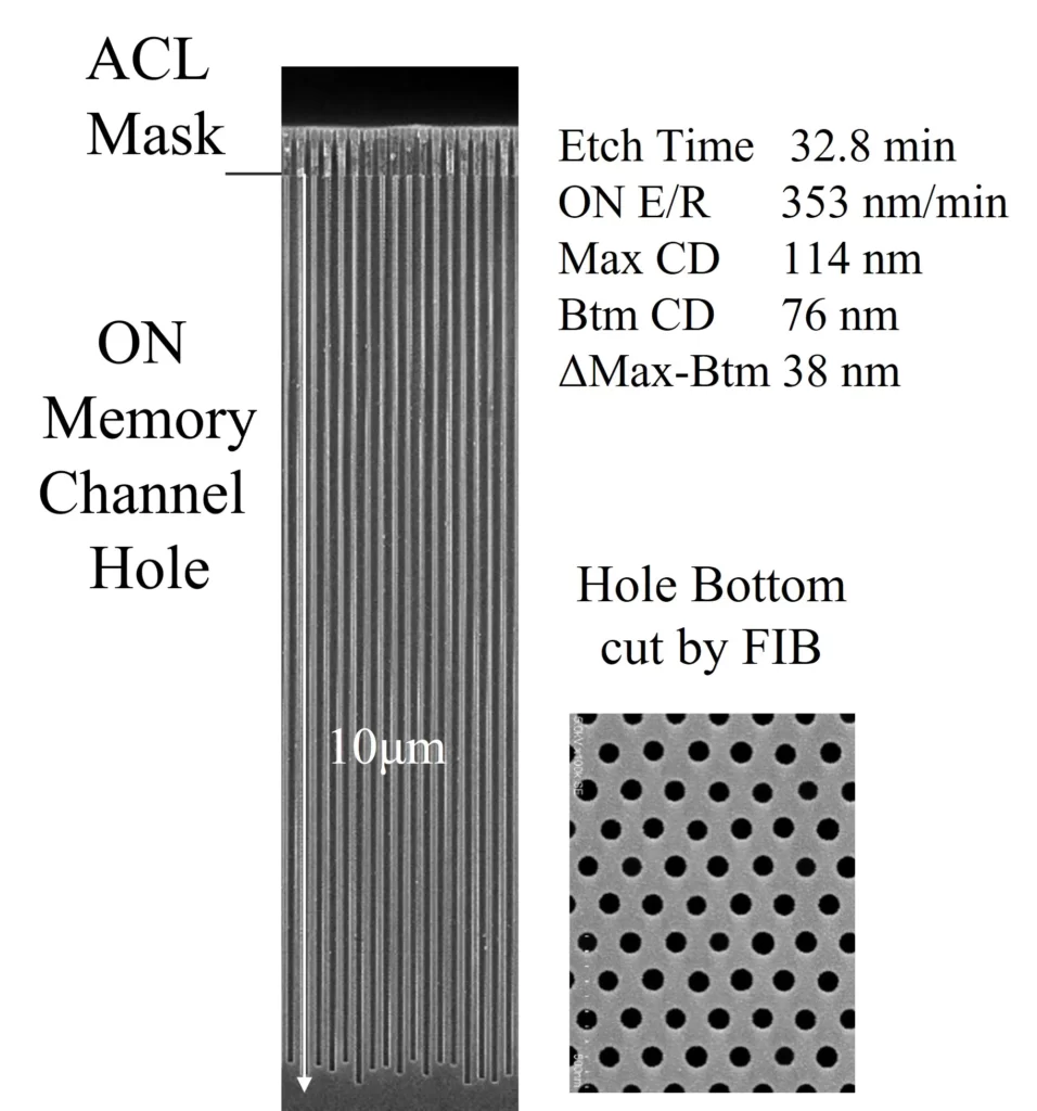
The newly developed process has brought dielectric etch application to the cryogenic temperature range for the first time. It thus produced a system with exceptionally high etch rates. Specifically, the innovative technology enables a 10-µm-deep etch with a high aspect ratio* in just 33 minutes. Also, it can reduce the global warming potential by 84% compared to previous technologies. Additionally, the geometry of the etched structure is quite well-defined as shown in the Figure 1. The potential innovations enabled by this technology will spur creation of 3D NAND flash memory with even larger capacity.
The development team at TEL is set to present a report on its research results at the 2023 Symposium on VLSI Technology and Circuits. Specifically, it is one of the most prestigious international conferences on semiconductor research, happening from June 11 to June 16 in Kyoto.
Continuing to pursue the motto of Best Products and Best Technical Service, TEL contributes to technological innovation in semiconductors. “As this year marks the 60th anniversary of our founding—which we consider to be a new transformative point for us—we will take on new challenges and continue to evolve, contributing to the development of a dream-inspiring society,” according to the company.
*Aspect ratio: Depth to width ratio of the pattern formed on the wafer.
- Share: