ASIA ELECTRONICS INDUSTRYYOUR WINDOW TO SMART MANUFACTURING
Sony’s Industrial Use CMOS Sensor to Propel Automation
Sony Semiconductor Solutions Corporation (SSS) has announced the upcoming release of the IMX900, a 1/3-type-lens-compatible, 3.2-effective-megapixel*1 stacked CMOS image sensor. Most importantly, it has a global shutter for industrial use that features the highest resolution*2 in its class.
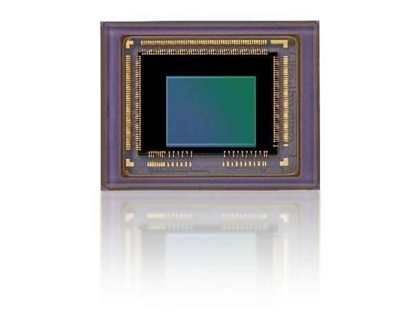
The new sensor product employs an original pixel structure to dramatically improve light condensing efficiency and near-infrared sensitivity. Thus, enabling the miniaturization of pixels while maintaining the key characteristics required of industrial image sensors. This design achieves the industry’s highest resolution*2 of 3.2 effective megapixels for a 1/3.1-type. In addition, a global shutter system that fits in the S-mount (M12), the mount widely used in compact industrial cameras and built-in vision cameras.
Helps Resolve Industrial Issues
The new product will contribute to the streamlining of industrial tasks in numerous ways. First, it serves applications such as code reading in the logistics market. Also, it assists in automating manufacturing processes using picking robot applications on production lines. Thus, helping to resolve issues in industrial applications.
Demand for automation and manpower savings are on the rise in every industry. For that reason, the original Pregius S™ global shutter technology of Sony Semiconductor Solutions contributes to improved image recognition. Thus, enabling high-speed, high-precision, motion distortion-free imaging in a compact design.
The new sensor utilizes a unique pixel structure developed based on Pregius S. Thereby moving the memory unit*3 previously located on the same substrate as the photodiode to a separate signal processing circuit area. This new design makes it possible to enlarge the photodiode area. Thus, enabling pixel miniaturization (2.25 μm) while maintaining a high saturation signal volume. Thus, successfully delivering a higher pixel count of approximately 3.2 effective megapixels for a 1/3.1-type sensor.

Wide Range of Applications
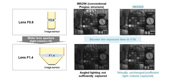
Moving the memory unit to the signal processing circuit area has also increased the aperture ratio. In short, bringing significant improvements to both incident light angle dependency*4 and quantum efficiency. These features enable a much greater level of flexibility in the lens design for the cameras that employ this sensor. Additionally, a thicker photodiode area enhances the near-infrared wavelength (850 nm) sensitivity and nearly doubles the quantum efficiency compared to conventional products. *5
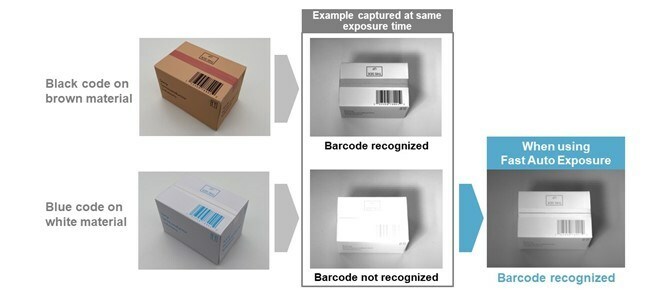
This compact, 1/3.1-type product is available in a package size that fits in the S-mount (M12), the versatile mount type used in industrial applications. It can be used in a wide range of applications where more compact, higher-performance product designs are necessary. Particularly, in compact cameras for barcode readers in the logistics market, picking robot cameras on production lines. Equally important are applications in the automated guided vehicles (AGVs) and autonomous mobile robots (AMRs) that handle transportation tasks for workers.
- Share: