ASIA ELECTRONICS INDUSTRYYOUR WINDOW TO SMART MANUFACTURING
Tokyo Electron Develops Extreme Laser Lift Off Technology
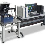
Tokyo Electron Limited announced that a development team at Tokyo Electron Kyushu, – the development and manufacturing site for wafer bonder/debonder systems- has developed an Extreme Laser Lift Off (XLO) technology. Specifically, it contributes to innovations in 3D integration of advanced semiconductor devices adopting permanent wafer bonding. This new technology suits two permanently bonded silicon wafers. Also, it uses a laser to separate the top silicon substrate from the bottom substrate with an integrated circuit layer.
The progress of digital society is raising expectations for greater improvement in semiconductor chip performance. As a result, next-generation semiconductors feature further scaling and higher integration. Also, they feature advancements in 3D integration using the permanent wafer-to-wafer bonding technology. In the current permanent wafer bonding sequence, two wafers with integrated circuits on their surface are permanently bonded together before going through a grinding process. In this process, the top wafer is thinned and removed.
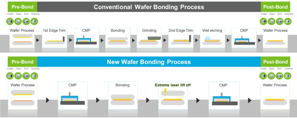
Advanced semiconductor devices require an increasing number of stack layers. As a result, there is a growing concern that the grinding process may decrease the yield due to factors such as the stress on wafers while grinding, delaminating of films after grinding, and widening of the edge trimming area (which reduces the number of viable chips on a wafer). For these reasons, technological innovation is required with a different approach from grinding technology.
TEL’s breakthrough Extreme Laser Lift Off technology replaces the current wafer thinning and removal process that relies on grinding. Accordingly, it enables the removal of the top silicon wafer without the yield concerns associated with the existing process.
Moreover, the Extreme Laser Lift Off technology simplifies the wafer thinning process by replacing and eliminating multiple existing steps. These include backside grinding, polishing and chemical etching of silicon wafer. Compared with the grinding process, the Extreme Laser Lift Off process does not require deionized water. Eventually, this leads to an over 90% reduction in water consumption and a significant drop in the drain water, thus lessening the environmental load. Furthermore, the company also develops a technology to properly treat and reuse the top silicon substrate separated by Extreme Laser Lift Off. It can help reduce the CO2 emissions from wafer fabrication.
Continually adhering to the motto of Best Products, Best Technical Service, TEL will keep contributing to technological innovation in semiconductors. As the company celebrated its 60th founding anniversary this year, this milestone becomes a new starting point for its further challenge and evolution to contribute to the development of a dream-inspiring society.
- Share: