ASIA ELECTRONICS INDUSTRYYOUR WINDOW TO SMART MANUFACTURING
TOPPAN Eyes New Facility for Semiconductor Packages
TOPPAN Inc., a TOPPAN Group company and a wholly owned subsidiary of TOPPAN Holdings Inc., will build a site to develop next-generation technology and construct a mass production line. Particularly, the planned site will produce Flip Chip Ball Grid Arrays (FC-BGAs) that meet the demand for high-speed transmission and chiplet1 use.
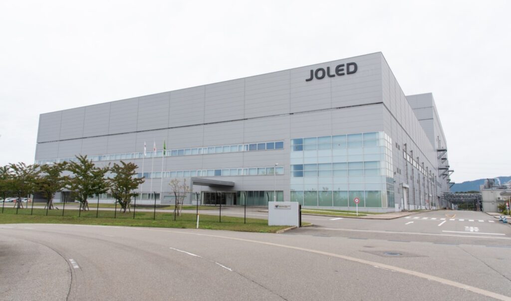
Accordingly, TOPPAN has entered into a sale and purchase agreement with JOLED Inc., an OLED manufacturer, for the land and buildings at the JOLED Nomi Site in Japan’s Ishikawa prefecture.
FC-BGAs are high-density semiconductor packages. Most importantly, the industry expects significant growth in this field due to increased demand. Particularly, coming from data centers and generative AI. TOPPAN expects to launch the new line in 2027 or thereafter. Moreover, it is also considering the production of its existing electronics products at the Nomi Site.
Background, Objectives
With society’s digitalization progressing at pace, the volume of data traffic is increasing every year. This is focusing attention on 2.xD packages2 and other next-generation semiconductor packages. Especially, those that responds to needs for high-speed, large-volume transmission.
TOPPAN is currently expanding FC-BGA production capacity at its Niigata Plant in Japan. However, there’s not much room for future expansion at its existing facility amid the face of fierce demands. Thus, the company has therefore been considering how to secure a new production base and identified the JOLED Nomi Site. Moreover, it sees this location to meet the requirements for next-generation semiconductor package manufacturing processes.
Sophisticated Factory Facility
TOPPAN will push forward with development of next-generation semiconductor package technologies and the construction of a mass production line expected to go live in 2027 or thereafter. TOPPAN will use digital twin,3 factory automation, and AI technologies to target the smooth launch of a state-of-the-art facility that reduces manpower needs and drives high production efficiency.
Notes:
1. Chiplet: A technology for providing large-scale circuits in a single package composed of multiple small individual chips.
2. 2.xD package: A semiconductor package featuring a fine wiring substrate called an interposer between the chip and the resin substrate.
3. Digital twin: A technology for digitally replicating the objects and data of a real space.
- Share: