ASIA ELECTRONICS INDUSTRYYOUR WINDOW TO SMART MANUFACTURING
Hitachi High-Tech Streamlines Materials Manufacturing
Hitachi High-Tech Corporation has conducted a proof of concept (PoC) trial using Chemicals Informatics (CI) and Materials Informatics (MI) to improve the efficiency of developing metal thin film materials used in electronic and other devices. Mainly, the PoC demonstrated an overall workload reduction of more than 80% even when developing new materials. The results show that the use of these tools is possible to streamline operations.
In recent years, MI has been increasingly used to reduce the amount of trial-and-error during the development of materials. Mainly, MI utilizes AI to derive the optimal combination ratio and composition of materials based on accumulated past experimental data. Meanwhile, CI is Hitachi High-Tech’s proprietary service that uses AI to analyze public data such as patents. Also, it selects optimal materials for development. Mainly, CI and MI contribute to the efficiency of development.
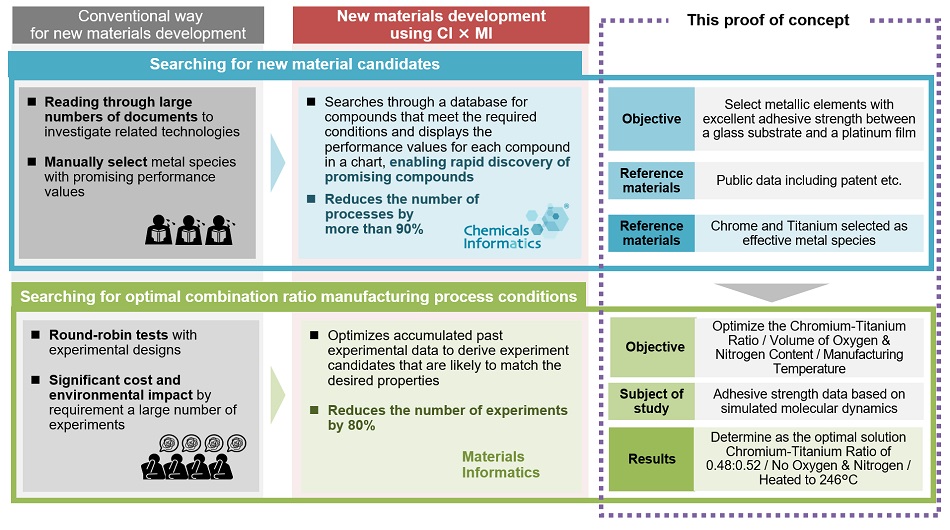
The PoC clarified that more efficient development even of new materials with no accumulated past experimental data is possible by combining Hitachi High-Tech’s MI with CI. This eliminates the document research and round-robin test with experimental designs*1, thereby improving the efficiency of developing new materials.
Hitachi High-Tech intends to offer the process of this PoC as a service for customers, primarily chemical and material manufacturers, whose demand for increasingly sophisticated and efficient development processes is escalating. The service will only improve the efficiency of development. Also, it will help to mitigate environmental impact by reducing the amount of experimentation required during the development process.
Background of the PoC
The demand for highly sophisticated materials is greater than ever for their functionality. Also, demand arises from their use to solve social issues such as achieving a carbon-neutral/decarbonized society. There is a rising need for digital transformation (DX) and green transformation (GX) to fundamentally strengthen R&D and improve operational efficiency. Therefore, many organizations have actively introduced MI as an AI-enhanced method of developing new materials. Specifically, MI is useful in fields where existing materials have already been developed. However, it cannot be used to improve efficiency when developing new materials, where there is no prior accumulated data to pull from during the selection of raw materials. As such, it needs a new tool.
Details of the PoC
This PoC tested the development of metal thin film materials used in electronics and other devices.
Metal thin films are created by depositing atoms onto substrates made from materials such as silicon or glass to form thin film layers. Lamination follows and then they are used to make electronic devices. A weak bond between the substrate and the metal thin film causes the film to peel away. This results in poor performance. Thus, strong adhesion is a key design consideration, but the design of adhesion needs many development process.
The PoC demonstrated a reduction of more than 80% in the number of development processes compared to conventional methods. It used CI to determine the most suitable metallic elements for the adhesion layers between substrates and metal thin films. Also, it used MI to determine the best combination ratios of metallic elements and the optimal conditions for manufacturing process.
- Using CI to select optimal materials based on patent data
Previously, selecting the ideal materials for development involved reading through extensive reference documentation. It allows finding the necessary information. Then, it conducts round-robin tests with experimental designs for all of the candidate materials to verify which one works best.
In this PoC, CI made the discovery of optimal material for a strong adhesive layer between a glass substrate and a platinum film. As information required for CI, we input 2 kinds of adherends – glass and platinum – and 30 kinds of metal elements. From 600,000 possible combinations, we extracted chromium, titanium, cobalt and yttrium as materials showing high adhesion strength data for both glass and platinum. Out of these four types, we narrowed it down to two types, chromium and titanium. We excluded cobalt and yttrium, which are expensive, considering the cost aspect. Then, we conducted just two experiments to verify the strength of the adhesive layer.
We factored in the time spent acquiring necessary information from reference documents and the number of verification experiments required. As a result, we were able to reduce the total number of processes by more than 90%.
2. Using MI to search for optimal conditions such as material combination ratios and manufacturing processes
In the past, determining optimal conditions for materials used in development involved numerous repeated experiments. These include ideal combination ratios, volumes and temperatures, However, MI makes it possible to determine such conditions efficiently. Specifically, it picked out candidates for required experimentation in advance based on past experimental data.
In this PoC, we used MI to research four optimal conditions required when designing the adhesive layer. This reduced the number of experiments required by approximately 80%. The results are in the table below.
Four optimum conditions in the adhesive layer:
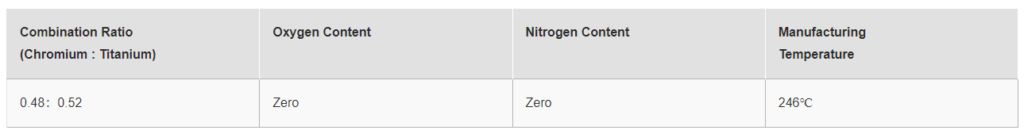
Based on the results of the above processes, we added an adhesive layer made of chromium-titanium alloy to the glass substrate at 246ºC when forming the platinum film. Then, we verified that peeling did not occur at room temperature or at a high temperature of 800ºC.
3. Reducing CO2 Emissions
By using MI and CI, the numbers of experimentations are reduced in a series of steps. These range from selecting optimal materials to searching for optimal conditions. So compared with conventional method, this process using MI and CI reduced the amount of CO2 emissions from 1.77 tons to 1.42 tons — a reduction of 0.35 tons*2. Thus, it contributes to carbon neutrality and decarbonization.
The company will present this content at the spring meeting of the Japan Institute of Electronics Packaging at Noda Campus of Tokyo University of Science on the 13th of March, 2024.
Hitachi High-Tech is providing solutions that contribute to resolving challenges faced by manufacturing companies, as well as working to create new social and environmental value and contributing toward the realization of a sustainable society.
*1 Experimental designs: A method of conducting experiments under a combination of conditions, using a combination of conditions to derive the necessary experiments without omission through statistics, and analyzing the results.
*2 Calculated based on the Guidance on Calculation and Reporting of Avoided Emissions issued by the WBCSD (World Business Council for Sustainable Development). The amount of reduction depends on the evaluation conditions and the evaluation model.
- Share: