ASIA ELECTRONICS INDUSTRYYOUR WINDOW TO SMART MANUFACTURING
GF Secures $1.5B Funding from U.S. Govt
The U.S. Department of Commerce has announced US$1.5 billion in planned direct funding for GlobalFoundries (GF) as part of the U.S. CHIPS and Science Act. Accordingly, the investment will enable GF to expand and create new manufacturing capacity and capabilities.
This will help in securely producing more essential chips for automotive, IoT, aerospace, defense, and other vital markets.
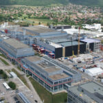
New York-headquartered GF is the only U.S.-based pure play foundry with a global manufacturing footprint including facilities in the United States, Europe, and Singapore. GF is the first semiconductor pure play foundry to receive a major award (over $1.5 billion) from the CHIPS and Science Act. Moreover, they aim to strengthen American semiconductor manufacturing, supply chains and national security. The proposed funding will cover three GF projects.
Projects in the Pipeline
The funding will cover expansion of GF’s existing Malta, NY, fab. Particularly. Particularly, by adding critical technologies already in production in GF’s Singapore and Germany facilities for U.S. auto industry. This expansion will ensure supply chain resilience for the growing demand. At the same time, to deliver GF’s automotive customers including General Motors. This will continue to diversify GF’s flagship Malta fab into new technologies and end markets.
Next, the planned funding will also enable construction of a new state-of-art fab on the Malta campus to meet expected customer demand for U.S.-made essential chips. Particularly, covering across a broad range of markets and applications including automotive, aerospace, defense and AI.
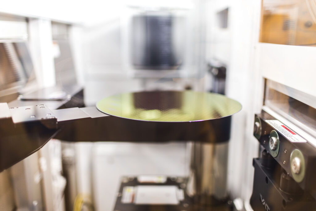
The new fab, which has already been granted some necessary permitting, will leverage the site’s existing infrastructure and ecosystem. Thus, enabling a fast and efficient path from construction to production. GF’s new fab will be uniquely positioned to capture the feature-rich mature, essential chip segment which is expected to continue to represent more than 60% of the semiconductor market. Construction of this new fab combined with expansion of GF’s existing site will likely triple the existing capacity of the Malta campus over the next 10+ years. These two projects are expected to increase wafer production to 1 million per year once all phases are complete.
Moreover, the U.S. government funding will also help modernize GF’s longest continuously operated fab. Most importantly, it will cover the nation’s first and largest trusted 200mm facility in Essex Junction, Vermont. The project will upgrade existing facilities, expand capacity as well as create the first U.S. facility capable of high-volume manufacturing of next-generation gallium nitride (GaN) semiconductors.
Based on market requirements and demand, GF plans to invest more than $12 billion over the next 10 plus years across its two U.S. sites through public-private partnerships.
These investments will create over 1,500 manufacturing jobs and about 9,000 construction jobs over the life of these projects.
- Share: