ASIA ELECTRONICS INDUSTRYYOUR WINDOW TO SMART MANUFACTURING
Applied Materials Preps up for Angstrom Era Chipmaking
At the SPIE Advanced Lithography + Patterning conference, Applied Materials, Inc. introduced a portfolio of products and solutions designed to address the patterning requirements of chips in the “angstrom era.”
Today, chipmakers transition to process nodes at 2nm and below. Thus, they increasingly benefit from new materials engineering and metrology techniques that help overcome EUV and High-NA EUV patterning challenges. Among them include line edge roughness, tip-to-tip spacing limitations, bridge defects and edge placement errors.
Sculpta Momentum: Growing Adoption and New Applications
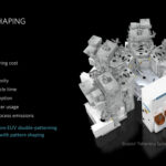
At last year’s SPIE lithography conference, Applied introduced the Centura® Sculpta® patterning system. Particularly, it allows chipmakers to reduce EUV double patterning steps by elongating patterned features. Accordingly, it brings the tips of the features closer together than achievable with a single EUV or High-NA EUV exposure. Applied is now working with all leading-edge logic chipmakers on a growing number of Sculpta applications. For example, in addition to reducing tip-to-tip spacing, chipmakers are using Sculpta to remove bridge defects; thereby enabling reduced patterning cost and improved chip yield.
“Leading chipmakers are seeing excellent results as they deploy Sculpta systems in production and explore additional applications beyond EUV double patterning step reduction,” said Dr. Prabu Raja, President of the Semiconductor Products Group at Applied Materials. “Sculpta is an entirely new tool in the patterning engineer’s tool kit that will be used in many more applications as engineers use their imaginations to solve challenging problems in new ways.”
“Pattern shaping is an innovative solution that is helping Intel accelerate its process technology roadmap,” said Ryan Russell, Corporate Vice President for Logic Technology Development at Intel. “We are deploying Sculpta systems for our angstrom process nodes, with initial results showing improved throughput, enhanced wafer yield, and reduced process complexity and cost. Pattern shaping facilitates new strategies for advanced patterning and paves the way for pushing lithographic print boundaries.”
“Pattern shaping is a breakthrough technology that addresses key challenges in the EUV era,” said Jong-Chul Park, Master of Foundry Etch Technology Team at Samsung Electronics. “Samsung is an early development partner and is evaluating the Sculpta systems for our 4nm process. We are looking forward to positive results, including reduced cost and complexity and increased yield.”
New Etch Technology Heals EUV Line Edge Roughness
EUV systems produce fewer of the photons needed to crisply define line and space patterns in photoresists. Accordingly, lines with rough edges are etched into the wafer, potentially creating open and short circuits in the chip. These yield-killing defects are becoming more prevalent as chipmakers implement angstrom era designs with narrower line and space patterns.
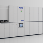
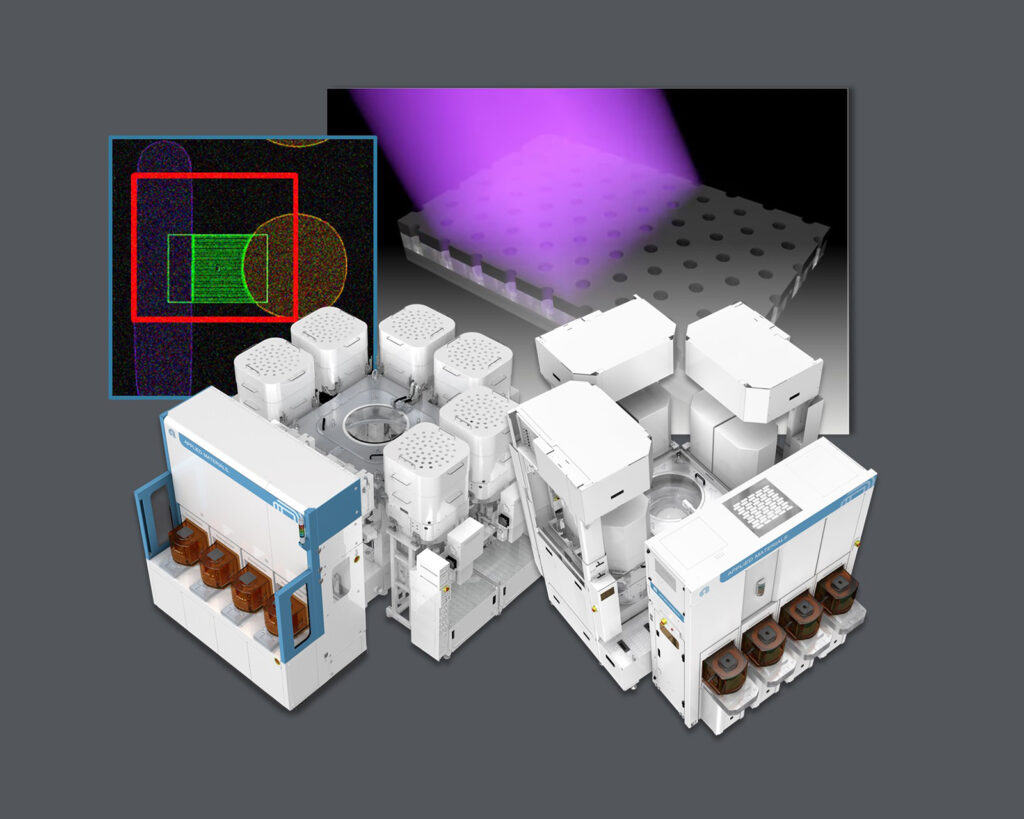
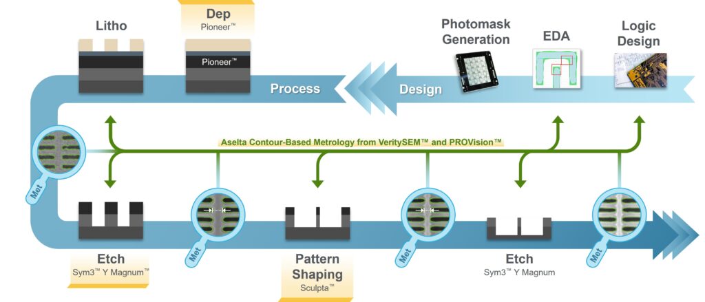
This time, Applied introduces the Sym3® Y Magnum™ etch system, which combines deposition and etch technology in the same chamber. The unique system deposits material along rough edges. This makes EUV line patterns smoother before they are etched into the wafer. Thus, it enables an increase in yields and a decrease in line resistance to improve chip performance and power consumption. In foundry-logic, Sym3 Y Magnum has already been adopted for critical etch applications at leading chipmakers. Now, it is being deployed for EUV patterning in angstrom era nodes. In memory, Sym3 Y Magnum is the most widely adopted etch technology for EUV patterning in DRAM.
New CVD Patterning Film for Angstrom Era Patterning
Additionally, Applied introduces the Producer® XP Pioneer® chemical vapor deposition) (CVD) patterning film. Specifically, the Pioneer film is deposited on the wafer prior to photoresist pattern processing. It is uniquely designed to transfer desired patterns to the wafer with exceptional fidelity. Pioneer is based on a unique high-density carbon formula more resilient to etch chemistries in most-advanced process nodes. This permits thinner film stacks with superior sidewall feature uniformity. Leading memory manufacturers for DRAM patterning already adopted the Pioneer film.
Pioneer has been co-optimized with Applied’s Sculpta pattern-shaping technology. Thus, it enables patterning engineers to maximize pattern elongation while maintaining tight control of the original EUV pattern. The patterning film is also being co-optimized with the new Sym3 Y Magnum etch system to provide higher selectivity and better control over conventional carbon films for critical etch applications in logic and memory processing.
Avoiding Placement Errors: Introducing Aselta
Applied’s industry-leading eBeam metrology systems are used by leading logic and memory companies to develop and control their most critical EUV patterning applications. A major challenge is tightly defining and placing the billions of features on each layer. Thus, they properly align with their opposite features on the next layer of the chip. Small placement errors reduce chip performance and power consumption, and large errors create yield-killing defects.
Applied has acquired Aselta Nanographics, a technology leader in design-based metrology using contours. Contours enable patterning engineers to gather orders of magnitudes more data about the shapes their recipes are creating in patterning films and on the wafer. This data is fed back into the lithography and process flow to create more exact on-chip features and placement.
“Aselta contour technology is now being integrated with Applied’s VeritySEM® CD-SEM system and PROVision® eBeam metrology system. It aims to give chipmakers a unique end-to-end capability that addresses the full spectrum of angstrom era metrology challenges,” said Keith Wells, Group Vice President of Imaging and Process Control at Applied Materials.
A Growing Patterning Portfolio and Business
Since 2012, Applied Materials has made patterning a research and development priority. It invested to deliver new products and solutions that help customers overcome their toughest patterning challenges. Particularly, this targets emerging EUV and High-NA EUV applications.
Today, the company’s patterning product portfolio includes CVD and ALD deposition; four types of materials removal (etch, selective materials removal, pattern shaping and CMP); thermal processes; and eBeam metrology. Also, it has increased its served available market in patterning from around $1.5 billion in 2013 to more than $8 billion in 2023. Additionally, it has grown its share of the opportunity from about 10 percent to more than 30 percent over the same timeframe.
- Share: