ASIA ELECTRONICS INDUSTRYYOUR WINDOW TO SMART MANUFACTURING
Applied Materials' Pattern-Shaping Technology Eases Chipmaking
Applied Materials, Inc. unveils a breakthrough in patterning technology. Specifically, the new system allows chipmakers to create high-performance transistors and interconnect wiring with fewer extreme ultraviolet (EUV) lithography steps. This discovery lowers the cost, complexity, and environmental impact of advanced chipmaking.
Customers increasingly use EUV double patterning to print chip features smaller than the resolution limits of EUV. This strategy aims to optimize chip area as well as cost. Chipmakers split a high-density pattern in half using EUV double patterning. As a result, they produce two masks that adhere to the resolution limits of EUV. Both halves of the pattern are combined on intermediate patterning films and then etched into the wafer. Double patterning is effective at increasing feature density. However, it adds design and patterning complexity along with process steps that consume time, energy, materials, and water. Moreover, it increases the cost of wafer fabs and wafer production.
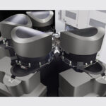
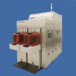
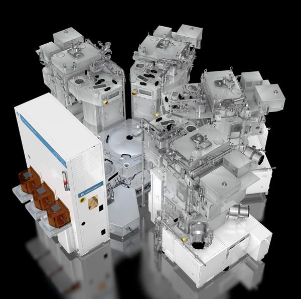
Applied Materials Centura® Sculpta® Patterning System
Applied Materials worked closely with leading customers to develop the Centura Sculpta patterning system. This development aims to help chipmakers continue shrinking designs without the added cost, complexity, and energy and materials consumption of EUV double patterning. Now, chipmakers can print a single EUV pattern. They can use the Sculpta system to elongate the shapes in any chosen direction to reduce the space between features and increase pattern density. The final pattern is created from a single mask, thus reducing design cost and complexity. Additionally, it eliminates the yield risk from double-patterning alignment errors.
EUV double patterning requires a number of added manufacturing process steps. Generally, they include CVD patterning film deposition, CMP cleaning, photoresist deposition and removal, EUV lithography, eBeam metrology, patterning film etching, and wafer cleaning. For each EUV double patterning sequence it replaces, the Sculpta system provides chipmakers with capital cost savings of approximately US$250 million per 100K wafer starts per month of production capacity; that translates to manufacturing cost savings of approximately US$50 per wafer. Also, the Sculpta system provides energy savings of more than 15kwh per wafer. This is equivalent to direct greenhouse gas emissions reduction of more than 0.35kg of CO2 per wafer. Moreover, it contributes approximately 15 liters of water savings per wafer.
“The new Sculpta system is a great example of how advances in materials engineering can complement EUV lithography to help chipmakers optimize chip area and cost while also tackling the growing economic and environmental challenges of advanced chipmaking,” said Dr. Prabu Raja, Senior Vice President and General Manager of the Semiconductor Products Group at Applied Materials.
“The Sculpta system’s unique pattern-shaping technology combines Applied’s deep expertise in ribbon-beam and materials removal technologies. Thus, it creates a breakthrough innovation for the patterning engineer’s toolkit,” continued Dr, Raja.
Customer and Industry Comments
“As Moore’s Law drives us to ever-greater compute performance and density, pattern shaping is proving to be an important new technology that helps reduce manufacturing cost and process complexity, and conserve energy and resources,” said Ryan Russell, corporate vice president for logic technology development at Intel Corp. “Having collaborated closely with Applied Materials in the optimization of Sculpta around our process architecture, Intel will be deploying pattern-shaping capabilities to help us deliver reduced design and manufacturing costs, process cycle times and environmental impact.”
“Three critical issues must be considered when pushing the limits of patterning: tip-to-tip spacing, pattern bridge defects, and line edge roughness,” said Jong-Chul Park, Master of Foundry Etch Technology Team at Samsung Electronics. “As an early development partner on the innovative pattern-shaping technology, I believe Applied’s Sculpta system is a fascinating breakthrough that addresses these patterning challenges and reduces manufacturing costs for chipmakers worldwide.”
“Applied Materials’ new Sculpta system is a revolution in patterning that brings an entirely new capability to chipmakers,” said Dan Hutcheson, Vice Chair, TechInsights. “The industry keeps pushing the limits of chip scaling. Thus, we need breakthroughs like Applied’s pattern-shaping technology that improves chip power, performance, area, and cost while also reducing design cost, and energy and materials consumption. Sculpta is the most innovative new process step in wafer fabrication since the introduction of CMP.”
The Sculpta system is receiving high interest from leading chipmakers. It has been selected as a production tool of record for multiple steps in high-volume logic manufacturing.
- Share: