ASIA ELECTRONICS INDUSTRYYOUR WINDOW TO SMART MANUFACTURING
SiGen 3DIC Transfer Aims at Interconnect Network Layers
Silicon Genesis (SiGen) extends its NANOCLEAVE™ Layer Transfer Process Technology for 3DIC integration using Interconnect Network Layers (INL) with device-scale metallization as the next step after 2.5D Redistribution Layer (RDL) packaging.
The proliferation of multi-chip packaging, generally referred to as 2.5D packaging, is limited by several factors. In the present state-of-the-art inter-chip metal connections, many forms of RDLs are available but in limited numbers of formats. Also, they are implemented with metal line widths significantly larger than fine features of present-day BEOL IC device connections. Additionally, current RDL interconnect feature scales restrict higher signal bandwidths in the 2.5D packages.
Moreover, due to the limited number of Interposer and RDL fabricators worldwide, the evolution to new composite chip systems using this approach will be much slower. Thus, it poses risks for bottlenecks in high volume production.
When Silicon Genesis NanocleaveTM methods for 3DIC integration are used for making INLs, many of the present-day RDL limitations are markedly reduced.
Layer Transfer for 3DICs and INLs
In applying the SiGen NanocleaveTM LT methods for 3DIC, Hydrogen protons are implanted through already formed transistors and related semiconductor elements. Among them are photodiodes for CIS devices. Using ≈200 keV ions, the range of protons in typical device structures provides a cleave plane depth ranging from 1 to 2µm.
A variation in use for NanocleaveTM LT methods allows for a shift from using 2.5D packaging RDLs in Silicon interposers or organic material bridges to using SiGen INLs that would match device-scale fine line geometries used in BEOL processing.
In addition to transferring complete CMOS device layers, LT can also be used to form standalone components of 3DIC stacks; in particular, cross-die and intra-die connections (functionally similar to RDLs used in 2.5D packaging) with device-scale metal and low-k dielectric structures.
The principal objectives for advanced packaging are to combine heterogeneous IC and other electrical and photonic components into functional systems with high-bandwidth internal connections, high reliability and lower cost. High-bandwidth signals depend on the number of internal connections provided by the packaging for data transfers.
Fundamental measures of signal transfer capabilities are the physical scale and density of these interconnects. For 2.5D packaging, including multi-chip “bridges”, such as Intel’s Embedded Multi-Die Interconnect Bridge (EMIB) technology, the metal line width and thickness used for RDL and equivalent connections ranges from several microns to tens of microns.
Formation of Metal and Dielectric INLs
A key aspect of the SiGen INL is the use of metal layer dimensions that closely approximate IC logic device interconnects. INL metal thickness and contact pitch range from ≈100nm to ≈200nm. They are almost 10 times smaller than metal lines used in typical RDL interposer and bridge structures in present-day 2.5D packaging.
The device-scale features used in fabricating INLs provide for: (1) smaller feature size metal line connections for higher bandwidth data rates and more precise timing connections across the 3DIC stack, (2) fabrication with standard BEOL methods and tool sets, and (3) fabrication of fine-feature connections across 3DIC structures larger than typical reticle sizes. INLs in standalone applications can be hybrid bonded to the 3DIC layers to provide both high-bandwidth vertical and extended range lateral connections.
Standalone INL Example
As an example of fabrication of a standalone INL by LT methods, consider a model metal network assembled from M1 to M4 from a 32nm logic BEOL stack of metal contacts and interconnects with low-k dielectric insulation layers. The M1 and M2 metal lines provide dense, high-bandwidth contacts for the INL. Meanwhile, the thicker M4 metal lines provide lower resistance, long-range lateral connections across the 3DIC stack dimensions (See Figure 1).
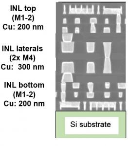
CMOS logic circuit. The INL is fabricated on a Si substrate by 32 nm node capable BEOL tool sets. The
total thickness of Cu metal lines in this model example is 700 nm.
The fabrication of the model INL is completed with the addition of selected dielectric layers on the top of the INL stack to prepare oxide and metal lines for high-bandwidth hybrid bonding to one layer of a 3DIC device stack. Prior to hybrid bonding to the 3DIC stack, the INL is implanted with Hydrogen at an energy sufficient to place the cleave plane at a desired depth in the Si substrate (See Figure 2).
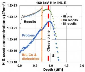
Hydrogen ions, placing the cleave plane at ≈0.2 um below the bottom surface of the INL layer.
After majority of the Silicon substrate is separated from the bonded INL structure by room temperature cleaving, the exposed bottom surface is prepared for hybrid alignment bonding to another layer in the 3DIC stack.
There are many other variations where LT methods can be used to fabricate 3DIC stacks of diverse die-scale and wafer-scale circuit elements. These include insertion of cross-die vertical and lateral high-bandwidth connections with either directly fabricated INL structures or bonded INL layers fabricated separately.
For additional details see US 11,410,984 B1, “Three Dimensional Integrated Circuit with Lateral Connection Layer”, issued: Aug 9, 2022.
- Share: