ASIA ELECTRONICS INDUSTRYYOUR WINDOW TO SMART MANUFACTURING
EV Group Revolutionizes 3D Integration with NanoCleave Layer Release Technology
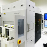
EV Group (EVG) has introduced NanoCleave™, a revolutionary layer release technology for silicon. NanoCleave enables ultra-thin layer stacking for front-end processing, including advanced logic, memory and power device formation, as well as semiconductor advanced packaging. It is a fully front-end-compatible layer release technology that features an infrared (IR) laser that can pass through silicon, which is transparent to the IR laser wavelength. Coupled with specially formulated inorganic layers, this technology enables an IR laser-initiated release of any ultra-thin film or layer from silicon carriers with nanometer precision.
As a result, NanoCleave enables silicon wafer carriers in advanced packaging processes such as Fan-out Wafer-level Packaging (FoWLP) using mold and reconstituted wafers as well as interposers for 3D Stacked ICs (3D SIC). At the same time, its compatibility with high-temperature processes enables completely novel process flows for 3D IC and 3D sequential integration applications. This enables hybrid and fusion bonding even of ultra-thin layers on silicon carriers; thereby revolutionizing 3D and heterogeneous integration as well as material transfer in next-generation scaled transistor designs.
Silicon Carriers Benefit 3D Stacking and Back-end Processing
In 3D integration, carrier technologies for thin-wafer processing are key to enabling higher performance systems with increasing interconnection bandwidth. Glass carriers have become an established method for building up device layers through temporary bonding with organic adhesives. They use an ultraviolet (UV) wavelength laser to dissolve the adhesives and release the device layers, which are subsequently permanently bonded onto the final product wafer.
However, glass substrates are difficult to process with semiconductor fab equipment that have been designed primarily around silicon, and that require costly upgrades to enable glass wafer processing. In addition, organic adhesives are generally limited to processing temperatures below 300°C, which limits their use to back-end processing.
Enabling silicon carriers with inorganic release layers avoids these temperature and glass carrier compatibility issues. In addition, the nanometer precision of IR laser-initiated cleaving opens up the possibility of processing extremely thin device wafers without changing processes of record. Subsequent stacking of such thin device layers enables higher bandwidth interconnects and opens up new opportunities to design and segment dies for next-generation high-performance systems.
Next-generation Transistor Nodes Demand Novel Layer-transfer Processes
At the same time, transistor roadmaps for the sub-3-nm node are calling for new architectures and design innovations. These include buried power rails, backside power delivery networks, complementary field-effect transistors (CFETs) and even 2D atomic channels, all of which will require layer transfer of extremely thin materials.
Silicon carriers and inorganic release layers support process cleanliness, material compatibility and high processing temperature requirements for front-end manufacturing flows. However, until now, silicon carriers had to be completely removed using grinding, polishing and etching processes, which results in micron-range variations across the surface of the working device layer. This makes the specific method unsuitable for thin-layer stacking at advanced nodes.
EVG’s new NanoCleave technology utilizes an IR laser and inorganic release materials to enable laser debonding on silicon with nanometer precision. This eliminates the need for glass substrates for advanced packaging, avoiding temperature and glass carrier compatibility issues. Also, it enables the ability to transfer ultra-thin (single micron and below) layers via carriers in front-end processing without changing the processes of record. The nanometer-precision of EVG’s new process supports advanced semiconductor device roadmaps calling for thinner device layers and packages, increased heterogeneous integration, and reduced processing costs through thin-layer transfer, and the elimination of glass substrates.
“Semiconductor scaling has become increasingly complex and difficult to achieve due to tighter process tolerances,” stated Paul Lindner, executive technology director at EV Group. “The industry needs new processes and integration approaches to enable higher integration density and device performance.
“Our NanoCleave layer release technology is a game-changer for semiconductor scaling through thin-layer and die stacking, with the potential to address the most pressing requirements of the industry. NanoCleave will help enable our customers to realize their advanced device and packaging roadmaps through a highly versatile and universal layer release technology that works with standard silicon wafers and wafer processes – enabling seamless integration in the fab and saving our customers both time and money,” continued Lindner.
Unique IR Laser Technology
Using EVG’s NanoCleave technology, the backside of the silicon wafer is exposed with an IR laser, which utilizes a unique wavelength that silicon is transparent to. An inorganic release layer that is pre-built into the silicon stack through standard deposition processes absorbs the IR light, resulting in the cleaving of the silicon at a predetermined and precisely defined layer or area. The ability to use inorganic release layers enables more precise and thinner release layers to be used (in the range of a few nanometers versus a few microns for organic adhesives). In addition, the inorganic release layers are compatible with high-temperature processing (up to 1,000 °C). This enables layer transfer for many new front-end applications, such as epitaxy, deposition and annealing, where organic adhesives are incompatible.
Product Availability
Demonstrations of EVG’s NanoCleave layer release technology are now available at the company’s headquarters.
Company executives will be available to discuss this IR laser transfer technology breakthrough at EMICON Taiwan, taking place at the Taipei Nangang Exhibition Center Hall 1 (TaiNEX 1) in Taipei, Taiwan, from September 14 to 16. Event attendees can visit EVG at Booth #L0316 (4th Floor) to learn more.
- Share: