ASIA ELECTRONICS INDUSTRYYOUR WINDOW TO SMART MANUFACTURING
Nanotronics Scales Wafer Inspection with Software Upgrade
Nanotronics, the factory control company bringing AI-powered inspection tools to manufacturing, announces the release of its latest nSpec™ software update, V 0.24.0.0. Specifically, the most recent upgrade provides users with both hardware and software capabilities critical to precision inspection of wafers, devices, and various samples.
Integrates Device Yield Analysis
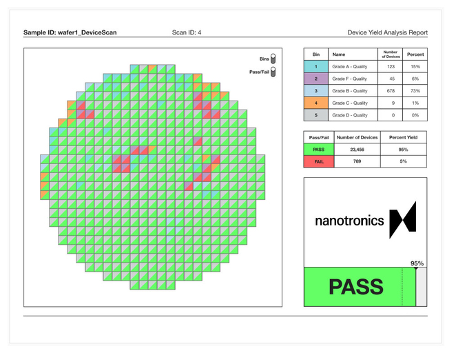
The new nSpec™ software integrates a new device yield analysis function. This way, Nanotronics enables manufacturers to easily calculate device yield as nSpec™ performs in-depth analysis for them. Subsequently, yield results are categorized according to device, allowing operators to view yield data from previous analyses. Also, this upgrade allows customers to develop a more thorough understanding of where device-killing defects are occurring according to their specified criteria. In implementing the device yield analysis, Nanotronics enables customers to maximize their investments in the nSpec™ platform, using intelligent machinery to scrap faulty wafers. Ultimately, they increase the ratio of working devices to the amount spent on production.
“Version 24 adds a brand-new device yield analysis capability, which improves automation with a simplified pass or fail output for sample devices. This removes the need for further operator inspection for sample quality,” says Chris Mallinson, Director of Software Engineering.
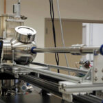
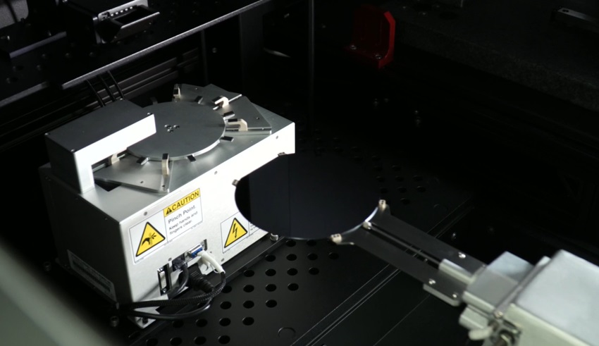
Additionally, Nanotronics has also made considerable hardware upgrades to the nSpec™ TURBO and nSpec™ CPS systems, which now include optional wafer handling solutions. Specifically, these capabilities accommodate front and back-side inspection of wafers, allowing for a more hands-free approach to performing full inspections. Manufacturers are now able to automatically flip wafers, scan, and characterize features of interest on both sides of the sample.
“The sample flipping capability expands automation to both sides of the sample, which cuts down on required operator intervention, possible human error, and condenses down the amount of necessary tool recipes,” adds Chris. “Combined with the device yield analysis, the two are sure to improve inspection throughput times so manufacturers can keep process lines moving as fast as possible without the worry of defective products.”
- Share: