ASIA ELECTRONICS INDUSTRYYOUR WINDOW TO SMART MANUFACTURING
FUJI's New 3D Printer Accelerates Development Process
FUJI Corporation has always been pursuing a wide range of technologies required for electronic component mounting. Particularly, aside from high-speed and high-precision mounting, the company also covers prototype boards with special shapes.
For that reason, the company is accelerating the introduction of new products for optimal production lines and meet diversifying customer needs.
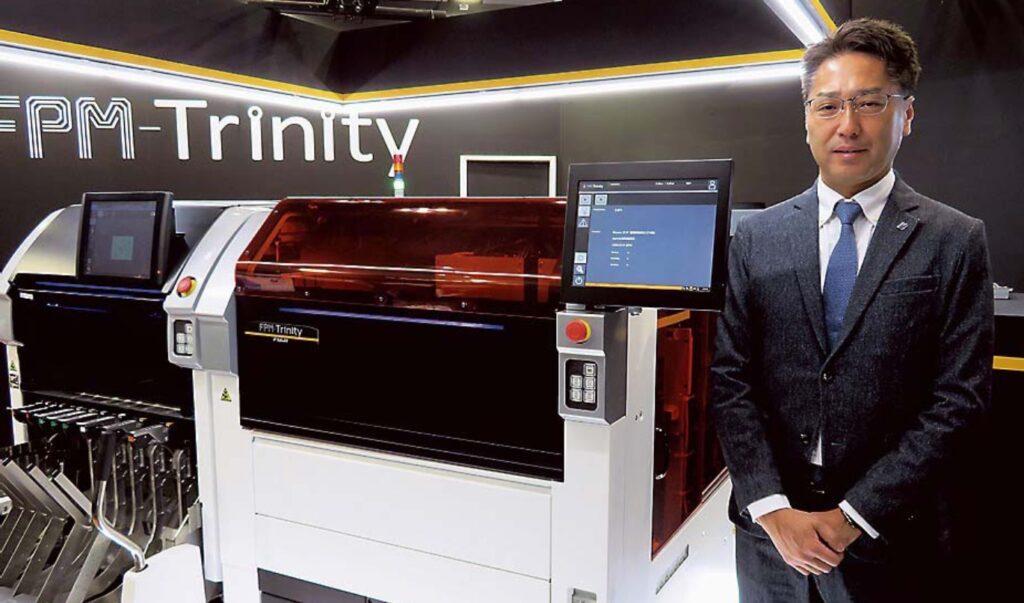
Recently, FUJI took part in INTERNEPCON JAPAN 2024 and took it as an opportunity to present its latest products and technologies. Specifically, the centerpiece was the FPM-Trinity, an electronics 3D printer under development.
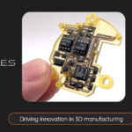
Unlike 3D printers that are already in practical use, the FPM-Trinity can complete multiple processes in a single unit. Particularly, from the formation of electronic circuits to the mounting of electronic components, in addition to the modeling of resin external shapes.
Amidst the growing awareness of sustainable manufacturing, the “Additive Manufacturing” method plays critical role in minimizing material loss. moreover, it reduces waste by layering and modeling materials. Along with rapid prototype substrate production, this method also contributes in reducing material loss and environmental impact.
Shortens Development Time
Joji Isozumi, President and COO of FUJI, said, “There has been a growing need, especially among European and US companies, to quickly produce prototype substrates to shorten development time. Unlike our conventional products used on electronic component mounting lines, FPM-Trinity equipment supports development. This is the most upstream part of the process,” he said.
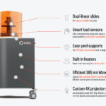
Furthermore, the FPM-Trinity manufacturing process involves printing resin ink, UV curing the resin, and printing silver nano ink to form circuits. This process repeats to create multiple layers and mount components. Resin formation has a maximum modeling size of 120 x 120 mm and a thickness of 4 mm.
Moreover, circuit formation has a minimum L/S of 140/200 micrometers and a thickness of 4 or 7µm. The maximum number of layers is 5. Applications include 3D shapes, circuit boards with built-in components, and a variety of other moldable objects.
FPM-Trinity uses FUJI’s proprietary advanced process to produce high-quality electronic devices. The resin has a higher glass transition point than general ultraviolet (UV) curable resins and has a lower rate of volume expansion in high temperature environments. Formation of circuit patterns is possible by repeated printing and drying using silver nano ink that can be sintered at low temperatures. It connects layers with a structure that forms circuits along the slope of the holes. Low-temperature curable silver paste is used for conduction instead of solder. Meanwhile, the underfill is filled around the component to ensure mechanical strength.
The company is developing a fully automated process to manufacture multi-layered boards, which is currently in the process verification stage.
–18 March 2024-
*The article is an English translation of an article published in the February 16, 2024 issue Dempa Shimbun Daily.
- Share: