ASIA ELECTRONICS INDUSTRYYOUR WINDOW TO SMART MANUFACTURING
Silicon Box Brings Smart Foundry to Italy in $3.6B Investment
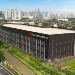
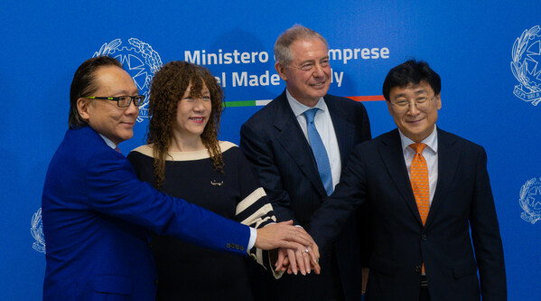
Silicon Box cutting-edge, advanced panel-level packaging foundry announced its intention to collaborate with the Italian government to invest up to $3.6B (€3.2B) in Northern Italy. Specifically, it will become the site for a new, state-of-the-art semiconductor assembly and test facility.
Moreover, this facility will help meet critical demand for advanced packaging capacity to enable next-generation technologies that Silicon Box anticipates by 2028. The multi-year investment will replicate its flagship foundry in Singapore, which has proven capability and capacity for the world’s most advanced semiconductor packaging solutions. Subsequently, it will expand further into 3D integration and testing.
When completed, the new facility will support approximately 1,600 Silicon Box employees in Italy. The construction of the facility will also create several thousand more jobs, including eventual hiring by suppliers. Design and planning for the facility will begin immediately. Also, construction will commence pending European Commission approval of planned financial support by the Italian State.
Silicon Box will bring the most advanced chiplet integration, packaging, and testing to Italy. Moreover, its manufacturing process is based on panel-level production. This is a world-leading, first-of-its-kind combination that is already shipping products to customers from its Singapore foundry. Through the investment, Silicon Box has plans for greater innovation and expansion in Europe, and globally. It will be a catalyst for broader ecosystem investments and innovation in Italy and other European Union nations.
“We believe innovation is driven by cultural values that embrace curiosity, passion, and a tireless commitment to excellence,” said Dr. Byung Joon (BJ) Han, co-founder and CEO of Silicon Box. “Italy was one of our top choices for global expansion because we found that its culture shares our values. We have seen great promise through our collaborations with the Italian government and various regional, institutional and commercial stakeholders to date, which we know will be necessary to successfully execute this first-of-a-kind project in Europe.”
“We are excited to bring Italy to the forefront of chiplet deployment and the semiconductor industry, through this investment into the world’s most advanced packaging solution. It will enhance competitive strengths in design, artificial intelligence (AI), large language models (LLMs), electronic vehicles (EVs) and automotive, mobile, wearables, smart consumer, edge computing, and material sciences of the Italian ecosystem, and revolutionize Europe’s position in the global [semiconductors] supply chain,” said Dr. Sehat Sutardja, co-founder and Chairman of Silicon Box. “Throughout my career, I have always been a big believer in Italian and European ingenuity.”
Advanced Packaging to Drive Innovation across Italian and European Semiconductor Ecosystems
“Italy was chosen as the location for Silicon Box’s first global expansion for several reasons, including its infrastructure, strong talent base and the government’s initiative to support and streamline the business environment and key stakeholder conversations,” said Dr. Han. “The competitive jobs that Silicon Box’s new facility will create will include engineers, equipment technicians, factory operators, and business functions. Italy offers an exceptional ecosystem for higher education with strong traditions in various engineering disciplines. This was a decisive factor in Silicon Box’s choice to build in Northern Italy and will be essential to our long-term success.”
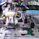
Wafer fabrication facilities, often referred to as “fabs”, create chips on silicon wafers through various advanced processes. Packaging facilities, such as the one planned for Italy by Silicon Box, receive completed wafers from fabs, cut them into individual chips, assemble or “package” them into final products and test them for performance and quality. The finished or packaged chips are then shipped to customers. Among them include specialty chip design companies, integrated device manufacturers (IDMs) and original equipment manufacturers (OEMs).
Notably, Silicon Box facilities specialize in advanced chiplet integration capabilities, on a large manufacturing format for scale. The chiplet concept is an alternative to traditional semiconductor manufacturing, which focused on building entire systems-on-chips (SoCs) on silicon wafers, then moving to conventional packaging processes. Chiplets describe the manufacture of individual system modalities as standalone chips or chiplets on a wafer. Thereafter, these separate functionalities are integrated into a system through advanced packaging, creating a system-in-package (SiP). With this, advanced packaging technology comes to the forefront of semiconductor manufacturing innovation, in a new paradigm for the industry.
The chiplet concept itself was introduced by Silicon Box co-founder Dr. Sutardja at the International Solid State Circuits Conference (ISSCC) in 2015, where he was a plenary speaker. Dr. Han is the inventor of semiconductor packaging solutions fundamental to enable chiplets through advanced packaging. Their collaboration has been the basis for Silicon Box’s record-breaking progress as a company in the semiconductor manufacturing space, traditionally dominated by a few large companies.
Bringing Resilience and Sustainability to the Semiconductor Supply Chain, and Enabling Advanced AI Technology and Ecosystems in Europe
“Silicon Box’s new foundry in Italy will be able to accept wafers from all foundries and support a wide variety of customers, worldwide, through its innovative approach,” said Mike Han, Silicon Box’s Head of Business. “The location is well suited to work with Europe’s existing and planned semiconductor wafer fabrication clusters in Italy, Germany, and France. Proximity will enable close collaboration from design through to final manufacturing. It will help increase resilience and cost efficiency of the European and global semiconductor supply chain, at a time when there is a global shortage for this type of technology.”
“Silicon Box’s investment in Italy can act as a catalyst for further investments by ecosystem companies and for building and attracting the talent needed to support a thriving European semiconductor industry,” co-founder Weili Dai said. “It will also enable existing Italian and European semiconductor interests to maximize their existing core competencies. Also, it will drive further efficiency and innovation through the creative and cost-efficient deployment of advanced packaging and chiplet architecture to support their own strategic objectives. This is particularly significant for the development of native artificial intelligence, large language models, supercomputers, mobile, wearables, smart factories, and edge computing companies.”
“This new Silicon Box AI-powered smart factory will be the first to showcase the ecosystem’s technology end-to-end. It ranges from initial design and construction to full process automation. Also, it highlights employee and customer training from our comprehensive digital twin. This will facilitate seamless expansion, employee and customer immersion, and groundbreaking efficiencies in management and performance monitoring,” she added.
Recent global disruptions emphasize the need to build a more resilient supply chain for semiconductors in Europe. Silicon Box supports the European Commission’s goal to reclaim 20 percent of global semiconductor manufacturing capacity by 2030. Also, it is committed to supporting a vision of a global semiconductor supply chain that is resilient and geographically balanced.
Silicon Box built its first advanced packaging facility in Singapore within a year. It began shipping finished products to customers three months after the factory’s grand opening. It showcased unique capability for fast project execution, which will also apply to the Italian factory.
Silicon Box’s products and practices are committed to sustainability and will adhere to high environmental standards across its global operations. This will also apply to Silicon Box’s first global facility in Northern Italy. Also, the facility will be constructed and managed according to Europe’s net zero principles. Therefore, it minimizes its carbon footprint and impact on the environment.
-18 March 2024 –
- Share: