ASIA ELECTRONICS INDUSTRYYOUR WINDOW TO SMART MANUFACTURING
Applied Materials Advances Heterogeneous Chip Integration
Recently, Applied Materials, Inc. introduced materials, technologies, and systems that help chipmakers integrate chiplets into advanced 2.5D and 3D packages using hybrid bonding and through-silicon vias (TSVs). The new solutions extend Applied’s industry-leading breadth of technologies for heterogeneous integration.
Mainly, heterogenous integration helps semiconductor companies combine chiplets based on a variety of functions, technology nodes, and sizes in advanced packages. Accordingly, it enables the combination to perform as a single product. Also, heterogenous integration helps solve industry challenges created in part because the need for transistors in applications, like high-performance computing and artificial intelligence continues to increase at an exponential rate while the ability to shrink transistors with classic 2D scaling is slowing and becoming more expensive. Moreover, heterogenous integration is a core component of a new playbook that enables chipmakers to improve chip performance, power, area-cost, and time to market (PPACt) in new ways.
Applied is the largest supplier of technologies for heterogenous integration with optimized chipmaking systems. These systems span etch, physical vapor deposition (PVD), chemical vapor deposition (CVD), electroplating, chemical mechanical polishing (CMP), annealing, and surface treatments.
“Heterogeneous integration is growing rapidly because it helps chip and systems companies overcome the limits of classic 2D scaling, which no longer delivers simultaneous improvements in performance, power, and cost,” said Dr. Sundar Ramamurthy, Group Vice President and General Manager of Heterogenous Integration (HI), ICAPS and Epitaxy, Semiconductor Products Group at Applied Materials. “Our latest HI solutions advance the industry’s newest ways to pack more transistors and wiring in 2.5D and 3D configurations to increase system performance, reduce power consumption, minimize size and speed time to market.”
Making Hybrid Bonds Stronger and Better
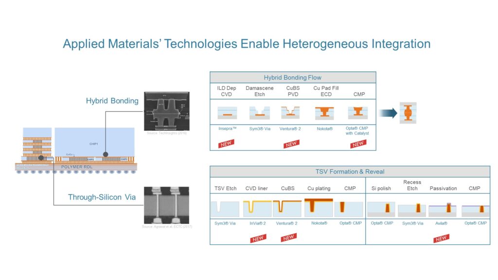
Chip-to-wafer and wafer-to-wafer hybrid bonding can be used to connect chips using direct, copper-to-copper bonds that enable the combined elements to perform as one. Hybrid bonding is the industry’s most advanced heterogenous integration technology in production today. Specifically, it improves throughput and power by packing more wiring into smaller spaces and reducing the distances signals need to travel.
Among the systems introduced are:
The Insepra™ SiCN deposition system expands Applied’s industry-leading hybrid bonding product portfolio. The system uses a new silicon carbon nitride (SiCN) material that delivers the highest dielectric bonding strength in the industry and offers superior copper diffusion barrier properties. The stronger dielectric bonds give designers the structural stability needed to integrate far more copper-to-copper interconnects in a given area, which lowers power consumption and increases device performance.
The Catalyst™ CMP solution helps customers control the amount of “dishing”. Specifically, it is the intentional recessing of copper material on two surfaces that will be bonded in a subsequent high-temperature annealing step. CMP dishing can create unwanted metal loss at the top surfaces of the copper pads, which can cause air gaps that decrease the fidelity and strength of the copper-to-copper bonds. Applied’s Catalyst solution is a dynamic temperature control technique that reduces dishing and increases throughput.
Bringing Through-Silicon Vias to New Heights
Used in high-volume manufacturing for more than a decade, TSVs are vertical wires used to precisely connect stacked chips. They are formed by etching trenches into silicon and then filling them with insulating liners and metal wires. As designers continue to integrate more logic, memory and specialty chips into advanced 2.5D and 3D packages, the number of TSV interconnects has expanded from a few hundred per package to thousands. To integrate more interconnects and accommodate taller stacks of chips, designers need the vias to become increasingly narrow and tall. Accordingly, this results in deposition uniformity variations that degrade performance and increase resistance and power consumption.
Further, Applied introduced new technologies for both dielectric and metal deposition. Specifically, these technologies enable higher-aspect-ratio TSVs and help chipmakers achieve their integration, performance and power goals:
The Producer® InVia® 2 CVD System is a new CVD process that makes dielectric liners uniform and electrically robust at the extreme aspect ratios needed by logic and memory customers in a growing variety of TSV applications. The InVia 2 system uses a propriety in-situ deposition process which enables excellent conformality for high-aspect-ratio TSVs. The system also offers higher throughput than ALD technologies, thereby reducing the per-wafer cost of TSV to help further expand its adoption.
The Endura® Ventura® 2 PVD System extends its widely adopted predecessor to TSV applications with aspect ratios of up to 20:1. The Ventura 2 system increases the control of metal TSV wire deposition to ensure a complete fill that delivers high electrical performance and reliability. The new TSV PVD process has been co-optimized for use with the Producer® InVia® 2 CVD process, giving customers a ready solution to their most challenging TSV designs. The Ventura 2 system is being deployed by all advanced foundry/logic chipmakers and all major DRAM producers.
The latest generation of Applied’s Producer® Avila® PECVD System is designed for TSV “reveal” applications. In the TSV process flow, wafers are bonded to temporary glass or silicon carriers and then thinned using CMP and etching to make the TSVs accessible. Following the TSV reveal steps, plasma-enhanced CVD technology is used to deposit a thin dielectric layer that electrically isolates the TSVs from each other. If the PECVD process generates heat above approximately 200o C, the delicate temporary bonding adhesive can be damaged, resulting in costly wafer yield loss. Applied’s Producer Avila PECVD system creates high-quality dielectric films at ultra-low temperatures and at high speed, meeting the low thermal budgets and high productivity required for TSV quality and cost.
- Share: