ASIA ELECTRONICS INDUSTRYYOUR WINDOW TO SMART MANUFACTURING
Device Isolation Processing of GaN on Si Power Devices
Gallium nitride (GaN)-based semiconductors are expected to supersede Silicon (Si) as the material for next-generation power devices and have been studied and developed together with Silicon Carbide (SiC) due to their excellent physical properties1). GaN-based semiconductors are already in practical use in the high-frequency device and power device fields, and the market is likely to expand further2). In particular, electronic devices such as GaN-HEMTs, which require low ON-resistance and high channel mobility, have been fabricated on Si substrates3), and production using ø6-inch and ø8-inch substrates is underway.
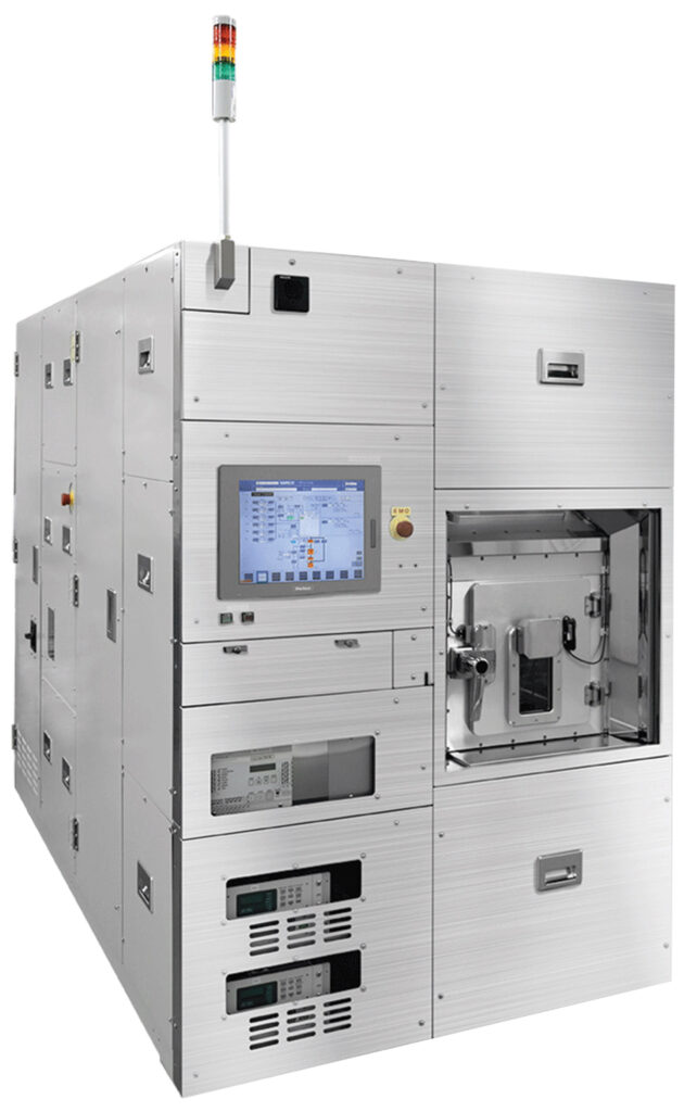
We provide ICP-RIE (Figure 1) and Chemical Vapor Deposition (CVD) systems and process technologies for GaN-based light-emitting devices, and have a proven track record in R&D and mass production. In this report, we introduce the device isolation process of GaN-based power devices formed on ø6-inch Si substrates using the RIE-800iPC ICP-RIE system for mass production.
Sample Structure and Processing Requirements
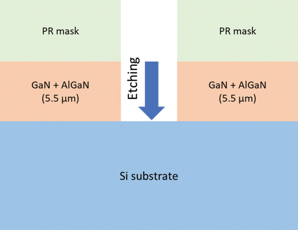
Figure 2 displays the actual processed sample structure where a photoresist (PR) is applied to a GaN and AlGaN layer (5.5µm) formed on a ø6-inch Si substrate, which is exposed and developed. The aperture area of the PR pattern is about 10%. Since the element isolation process is an etching process to reach the Si substrate, a degree of over-etching is required. However, excessive over-etching must be avoided, necessitating etching uniformity within the wafer.
Etching Endpoint Detection and Observation Results
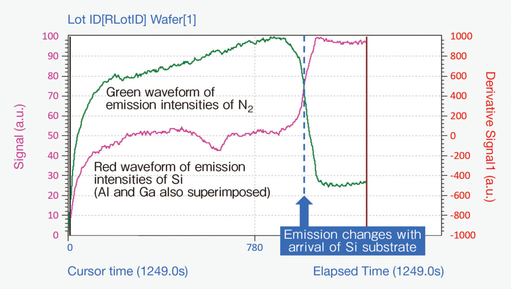
In order to strictly monitor the progress of over-etching, an optical emission spectroscopic endpoint monitor, which can accurately detect the endpoint using differences in material composition, was used in this report.
The measurement results from the endpoint monitor are shown in Figure 3. The green and red line waveforms represent the emission intensities of N2 and Si, respectively. After etching the GaN + AlGaN layer to reach the Si substrate, changes in emission intensities are evident as Si etching commences. In this instance, Si was over-etched for about one minute. Following over-etching, Si luminescence intensity (red line waveform) was detected consistently.
The SEM cross-sectional observation results of the etched ø6-inch full wafer are shown in Figure 4: after GaN + AlGaN (5.5μm) penetration, the Si substrate was over-etched by about 1.3μm as targeted, consistent with the emission spectroscopy observation results. A processing shape with a forward taper of about 40° was obtained. This is because the initial shape of the PR mask is about 60°, which is the target shape. To obtain a vertical shape, a vertical PR mask or a hard mask such as SiO2 can be used.
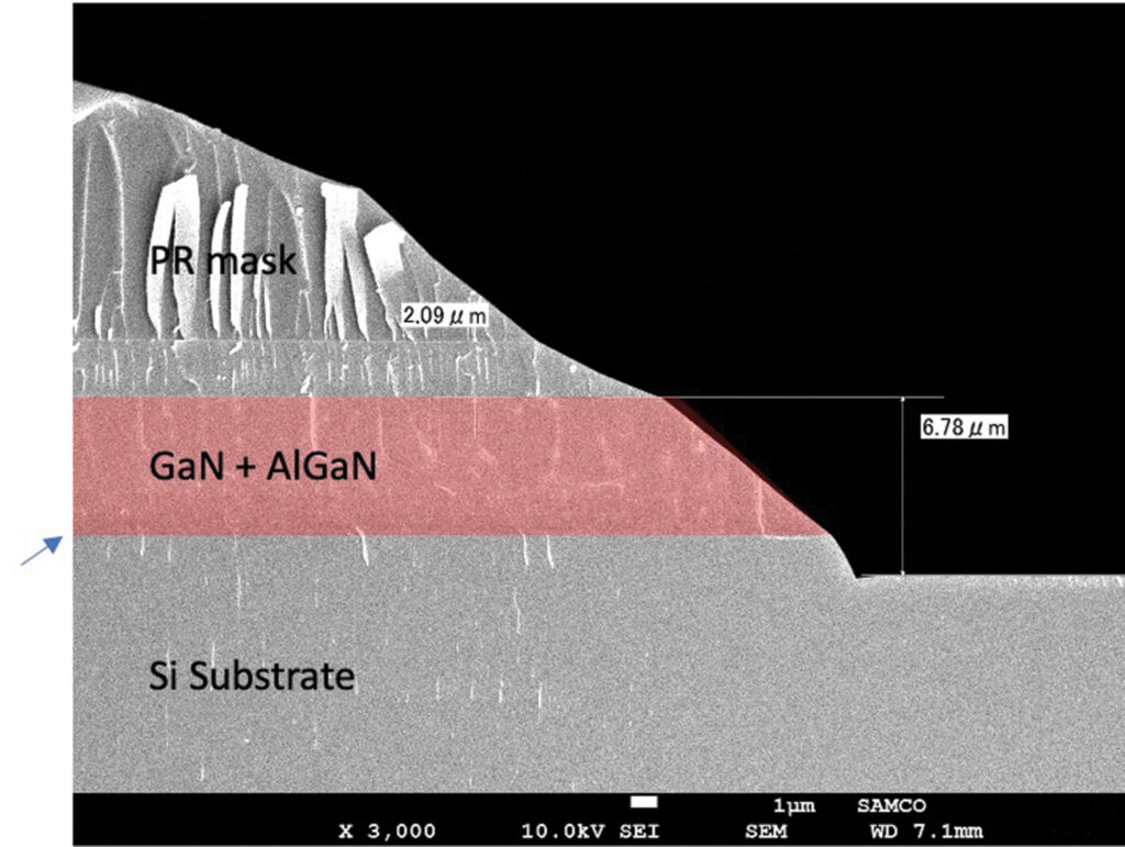
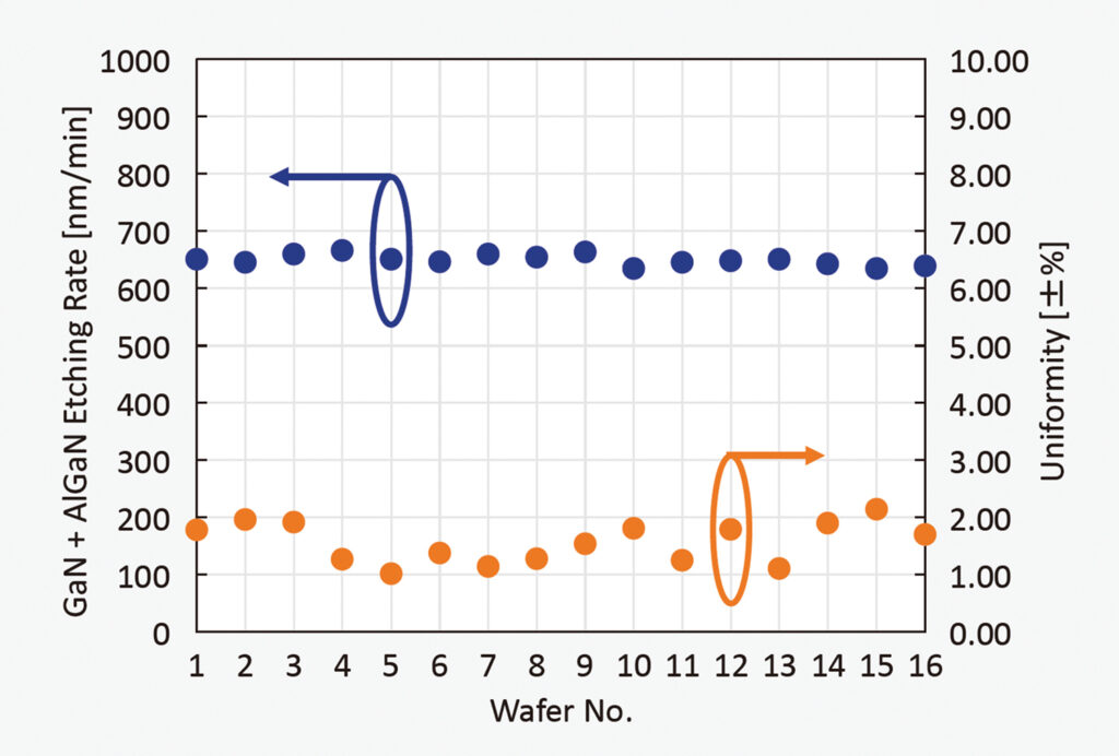
Figure 5 shows the results of continuous processing of 16 ø6-inch full wafers. The etching rate was stable at 600nm/min or higher, and all showed excellent in-plane uniformity of ±3% or less. The repeatability among the 16 wafers was ±2.46%, representing an impressive outcome. The etching rate was derived from the time the Si substrate was reached, as measured by an optical emission spectroscopic endpoint monitor. For in-plane uniformity, etching depths at five points (center and four peripheral points (5mm from the edge)) were measured with a step-measuring device.
Conclusion
The mass production ICP-RIE system, RIE-800iPC, demonstrated its proficiency in the separation and processing of GaN-based power devices. The RIE-800iPC, a production system with excellent process reproducibility, can not only etch GaN-based semiconductors, but also process compound semiconductors such as GaAs and InP, Si-based semiconductors such as SiO2 and SiN, ferroelectric materials such as PZT and Pt, metal materials, and resin materials such as polyimide. GaN-based power devices are key devices for realizing a low-carbon society. Our commitment to developing process technologies for GaN-based power devices contributes to this important societal goal.
References:
1) Jun Suda, Masahiro Horita, Kazutaka Kanegae. “Evaluation of point defects for realization of GaN vertical power devices.” JSAP 90.10 (2021): 628-631.
2) Kumazaki, Yusuke, et al. “Over 80% power-added-efficiency GaN high-electron-mobility transistors on free-standing GaN substrates. Physics Express 14.1 (2020): 016502.
3) Egawa, Takashi. “Growth of GaN single crystals on Si substrates and their device applications.” JSAP 81.6 (2012): 485-488.
-25 March 2024-
- Share:


About This Article:
The Process Development Department 1 from Samco, Inc. provided the contents of the article.