ASIA ELECTRONICS INDUSTRYYOUR WINDOW TO SMART MANUFACTURING
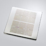
DNP Makes Photomask for 2nm EUV Lithography
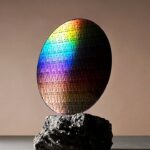
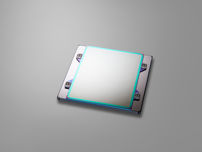
Dai Nippon Printing Co., Ltd. (DNP) has begun development of photomask manufacturing for 2-nanometer (10-9 meter) generation logic semiconductors that support extreme ultraviolet (EUV) lithography, the cutting-edge process for semiconductor manufacturing.
Also, DNP will act as a subcontractor and provide the newly developed technology to Tokyo-based Rapidus Corporation. Rapidus is participating in the Research and Development Project of the Enhanced Infrastructures for Post-5G Information and Communication Systems instigated by the New Energy and Industrial Technology Development Organization (NEDO).
Cutting-Edge Semiconductor Process
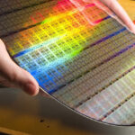
Generally, DNP has strengthened its ability to manufacture cutting-edge semiconductors with high productivity and quality. Specifically, in 2016, DNP was the world’s first merchant photomask manufacturer to introduce the multi-beam mask writing tool (MBMW).
In 2023, the company completed the development of a photomask manufacturing process for 3nm generation EUV lithography. Subsequently, it commenced development of 2nm generation technology. In response to the need for further miniaturization, DNP will begin full-scale development of a photomask manufacturing process for 2nm generation EUV lithography. It includes the operation of second and third multi-electron beam mask lithography systems in FY 2024.
Also, DNP plans to bring online its second and third MBMW mask lithography systems in FY 2024. This would accelerate the development of photomasks for 2nm generation EUV lithography.
Moreover, DNP will act as a subcontractor on Development of Advanced Semiconductor Manufacturing Technology (Commissioned) by Rapidus. This is part of the NEDO’s previously mentioned R&D project.
Sets Sights Beyond 2nm
By FY2025, DNP will complete the development of a manufacturing process for photomasks for 2nm generation logic semiconductors that support EUV lithography. From FY 2026 onwards, it will push ahead with the establishment of a production technology eyeing start of mass production in FY2027.
Moreover, the company has begun development toward the 2nm generation and beyond. Particularly, it has signed an agreement with imec, a cutting-edge international research organization headquartered in Leuven, Belgium, to jointly develop next-generation EUV photomasks.
DNP will continue to contribute to the growth of Japan’s semiconductor industry. It will promote development in collaboration with various partners within the framework of the international semiconductor industry.
-27 March 2024-
- Share: