ASIA ELECTRONICS INDUSTRYYOUR WINDOW TO SMART MANUFACTURING
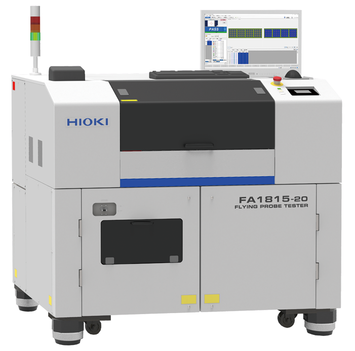
Hioki's New Probe Tester Offers Innovative Inspection
Hioki E.E. Corporation has introduced the FA1815-20 Flying Probe Tester(*1). Accordingly, the state-of-the-art solution enhances the inspection of high-density circuit boards crucial for the IT market.
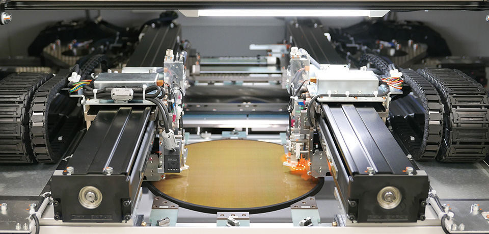
This innovative tester can inspect up to 100 points per second. Thus, offering high probing precision and insulation resistance(*2) inspections of up to 100GΩ at a test voltage of merely 10V. By ensuring rapid and high-quality testing of probe cards(*3) and other high-density boards, the FA1815-20 is set to significantly boost productivity in the semiconductor industry.
Background of development
Recently, there has been rapid advancement of new IT technologies. Specifically, the emergence of Artificial Intelligence (AI), the Internet of Things (IoT), 5G networks, and among others. For that reason, these megatrends are pushing the limits of electronic products worldwide.
As these technologies become increasingly integrated into society, the demand for failure-proof electronic products escalates. Furthermore, the core of these technologies, electronic circuits, require mounting on high-density boards. This is because semiconductor technology is becoming more complex and integrated. This trend needs more precise and comprehensive inspections to ensure reliability.
Innovating for the future
With remarkable progress in IT technology driving the semiconductor industry forward, reliability and productivity have become indispensable. Add to this, flying probe testers have long been the industry standard tool for PCB inspection. However, as inspection demands grow more stringent, the FA1815-20 emerges as the next-generation flying probe tester, ready to meet the challenges of precision and speed head-on.
Moreover, this tester introduces an innovative approach to insulation resistance inspection that minimizes some cautious users’ concerns about board damage with high-voltage testing in high-resistance inspections. Thus, this advancement represents Hioki’s commitment to providing market-leading solutions that contribute to societal progress.
Key features of the FA1815-20
Unmatched probing precision
The FA1815-20 achieves a probing resolution with a minimum pitch of 34 µm between patterns. Moreover, it can inspect circuit test pads as small as 4 × 4 µm square. This precision is essential for today’s increasingly fine circuit patterns.
Enhanced inspection speed
To address the challenges posed by the growing number of circuit patterns on high-density boards, the FA1815-20 comes with updated mechanical hardware. At the same time, it has a new probe movement algorithm. These improvements can reduce testing time by up to 30%(*4) compared to previous models, significantly enhancing productivity.
Eliminating concerns of damage to PCBs
Some cautious users may worry that high-voltage insulation resistance inspection may damage the PCBs. For that reason, the FA1815-20’s innovative head amp allows for inspections of up to 100 GΩ with at test voltage of only 10 V. This effectively eliminates concerns of damage to the boards in this inspection.
-5 April 2024-
Notes:
*1:Flying probe tester: These are devices that inspects circuit boards by rapidly moving measurement probes to test circuits across the board. They offer the flexibility to inspect substrates with varied patterns by presetting the position information and measurement parameters.
*2:Insulation resistance: This is the resistance between circuit patterns on a board. Low insulation resistance can lead to malfunctions and failures in electronic products.
*3:Probe cards: These are jigs used in the semiconductor production process, especially for Large Scale Integration (LSI) chips, for verification. for verification. Their base substrate consists of finely pitched patterns.
*4:Comparison in approx. 40,000 steps of continuity and insulation testing
- Share: