ASIA ELECTRONICS INDUSTRYYOUR WINDOW TO SMART MANUFACTURING
Siemens, Samsung to Offer IC Breakthrough in New Deal
Siemens Digital Industries Software and Samsung Foundry developed compelling new capabilities in manufacturing multi-die packaged designs at advanced nodes. Moreover, they also achieved a host of new product certifications for many of Siemens’ industry-leading IC design and verification technologies.
“Our expanded collaboration with Siemens EDA will help us deliver advanced design enablement solutions,” said Sungjae Lee, Vice President and head of Foundry PDK Development Team at Samsung Electronics. In addition, Lee said, “By aligning our roadmaps and optimizing the entire design flow, we can drive advanced packaging innovation across key markets like 5G, automotive, and AI.”
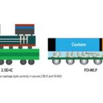
Siemens and Samsung: boosting 3D-IC manufacturability
Siemens and Samsung Foundry recently collaborated to update process design kits (PDKs). Specifically, this seamlessly integrates into Siemens’ Xpedition™ Substrate Integrator (XSI) software and Xpedition™ Package Designer (XPD) software. This is achievement that allows Samsung to deliver robust PDK updates to mutual customers with minimal disruption to design processes.
Siemens’ XSI software empowers engineers to construct a comprehensive digital twin model of an entire multi-die device. Thus, enabling seamless design integrations capable of driving all downstream design, analysis, verification, and signoff activities.
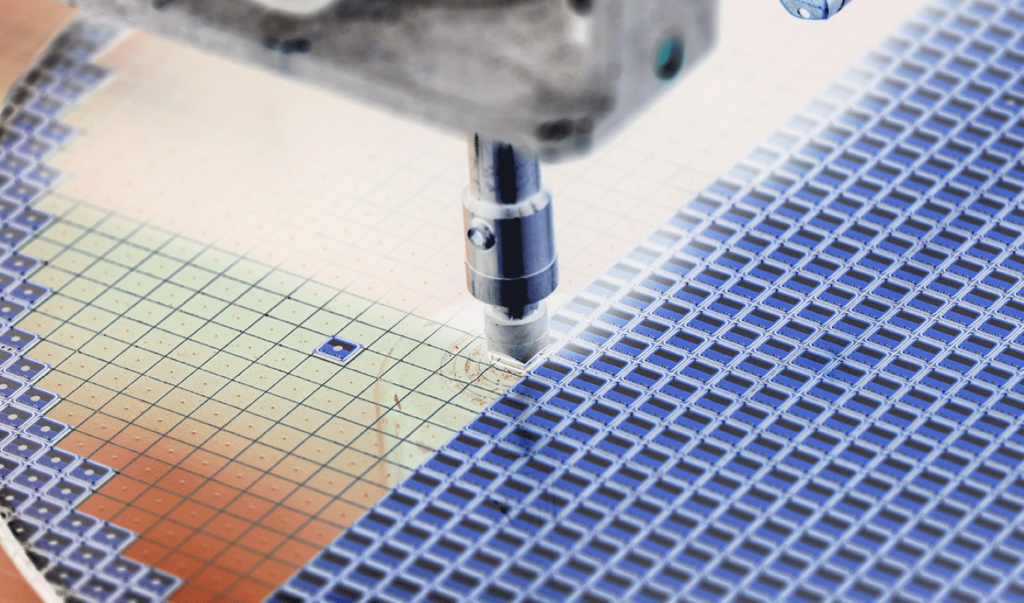
Samsung also successfully evaluated Siemens’ digitally integrated High Density Advanced Packaging (HDAP) flow for the foundry’s MDI (multi-die-integration) packaging process. Meanwhile, Siemens’ Calibre® xACT™ 3D software and Calibre xL parasitic extraction tools, which quickly and accurately extract register clock parasitics in complex 2.5D and 3D packaging configurations. They now come certified for Samsung’s most advanced process nodes, as part of Siemens’ larger Calibre® nmPlatform tool.
The parasitic extraction tools within Calibre support signal integrity-aware analysis of entire high bandwidth memory (HBM) channels implemented on 3.5D silicon interposers.
Moreover, Samsung has also qualified decks (4nm technology) for the dies with through silicon vias (TSV). Also, it validated the capability and accuracy of the Calibre parasitic extraction tools for TSV extraction and TSV coupling extraction tasks.
Samsung Certifies multiple Siemens EDA Product Lines, Reference Flows
Among the many additional recent achievements of the Siemens EDA/Samsung partnership are:
Siemens’ Calibre nmPlatform software for integrated circuit (IC) verification signoff. This includes Siemens’ new Calibre® DesignEnhancer software now fully certified for Samsung Foundry’s latest and greatest process technologies. Specifically, Samsung has qualified Siemens’ Calibre xACT parasitic extraction tool for the foundry’s multi-bridge-channel FET (MBCFET), an optimized version of Gate-All-Around (GAA) transistor technology. Siemens used novel methodologies for the efficient technology description and accurate extraction of parasitics of advanced transistor technologies beyond 3nm.
Samsung and Siemens have also leveraged AI-powered custom IC verification technologies such as Solido™ Design Environment and Solido Characterization Suite software to enhance variation-aware verification and characterization. Furthermore, the Solido™ Crosscheck™ software for comprehensive IP quality assurance.
Samsung has qualified Siemens’ Analog FastSPICE (AFS) platform for the foundry’s latest processes for SPICE accurate applications. Siemens’ AFS platform also comes certified across Samsung Foundry’s FinFET, Extreme UltraViolet (EUV) and GAA fabrication processes (SF4X, SF3P, SF2). Moreover, AFS has been qualified as well for Samsung Foundry’s fully depleted-silicon on insulator (FD-SOI) LN18FDS process technology. With these certifications, mutual customers can now verify their designs using Siemens’ AFS platform with SPICE accuracy and high performance.
Further Achievements of Partnership
Moreover, Samsung and Siemens have also successfully continued their collaboration around open model interface (OMI) development. Specifically, with Si2’s Compact Model Coalition (CMC). OMI, the industry-standard platform for enabling aging modeling and reliability analysis, has the support of Siemens’ AFS platform across Samsung Foundry’s processes from 14nm to 2nm.
Samsung has also certified Siemens’ Aprisa™ software for digital implementation for the foundry’s SF3P process node. With this certification, customers using Aprisa for digital implementation tasks can design projects at SF3P with fully certified technology, proven correlation with Siemens’ Calibre sign-off tools and support for all the design rules and features of Samsung Foundry’s advanced GAA process technology platform.
Further, Samsung and Siemens have created new design implementation solutions that improve power structure robustness and reduce design cycle time. Calibre DesignEnhancer, which is part of Siemens’ Shift Left initiative, takes the foundry’s rules and automatically performs layout optimization tasks that enhance the customer’s design. Calibre DesignEnhancer currently has three use models that use the Calibre platform to deliver DRC clean results, and multiple customers have successfully proven all three Calibre DesignEnhancer use models.
18 June 2024
- Share: