ASIA ELECTRONICS INDUSTRYYOUR WINDOW TO SMART MANUFACTURING
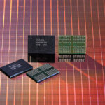
Samsung Begins Volume Production of 14nm DDR5 DRAM
Samsung Electronics has started volume production of 14nm DDR5 DRAM chips at its EUV, or extreme ultra violet lithography production line in what the chip maker said is the world’s finest ever of its kind.
Samsung said that it has applied the EUV lithography technology to pattern and etch out five layers to integrate more of transistors in silicon wafer in what’s called the industry’s highest density DRAM chips.
The upshot is a 20% gain in productivity, which translates into getting 20% more chips out of silicon wafer.
The chip shrinkage also translates into a 20% drop in the power budget, compared with the previous design rule.
The DDR5 is a next generation of DRAM specification that boasts of 7.2Gbps data transfer speed, double that of the predecessor DDR4.
As bandwidth-hungry applications like AI and deep machine learning are proliferating across the board, demand for DDR5 DRAM chips will boom soon in the datacenter, super-computer and corporate server markets.
Samsung believes that its ramp to the 14nm EUV lithography technology will advance the adoption of DDR5 specs across various market segments, because the productivity gain will make it more affordable.
With the commercial rollout of 24Gb DDR5 DRAM chips available on this 14nm EUV lithography platform, Samsung will lead the ramp up of DRAM chip market from DDR4 to DDR5.
- Share: