ASIA ELECTRONICS INDUSTRYYOUR WINDOW TO SMART MANUFACTURING
TEL to Soar Grit in IC Making With New Solutions
Tokyo Electron has launched a new gas cluster beam system designed to boost its prowess in EUV lithography. Moreover, the company has two single wafer deposition systems and a planned release for another in the future.
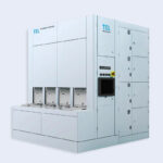
First, the company has announced the launch of AcreviaTM, a gas cluster beam system designed to modify ultra-fine patterns printed by EUV lithography. Subsequently, TEL also announced the release of single wafer deposition systems Episode 1 and Episode 2 DMR. Moreover, it confirmed the planned release of EpisodeTM 2 QMR down the road.
Contributes to Semiconductor Advancement
AcreviaTM is a gas cluster beam (GCB) system designed for modifying the critical dimensions and shape of ultra-fine patterns formed by EUV lithography. Thus, TEL’s unique GCB technology offers unprecedented low-damage processing and enables further device scaling. At the same time, the technology also offers yield improvement, and reduced EUV patterning costs for our customers.
AcreviaTM plays key role in the semiconductor manufacturing process flow following a single EUV lithography patterning and subsequent dry etching step. The patterned features irradiated with the directional gas cluster beam, which etches feature sidewalls at an optimal wafer tilting angle to modify critical dimensions and adjust ultra-fine patterns.
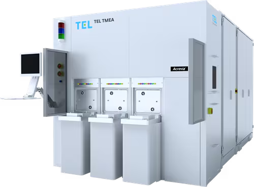
In addition, Acrevia’sTM precise wafer scanning system can control etch amount at any point on the wafer using TEL’s innovative Location Specific Processing (LSP) technology. Thus, resulting in unparalleled within wafer uniformity correction capabilities. AcreviaTM can also reduce line edge roughness (LER) on pattern sidewalls, and reduce stochastic litho defects to improve yield.
“Acrevia features our original technology that enables high etch rate and low damage patterning,” says Hiroshi Ishida, General Manager, DSS BU at Tokyo Electron. Furthermore, Ishida said, “In the increasingly challenging field of advanced patterning, Acrevia makes further scaling possible and maximizes productivity. Going forward, we will keep developing technologies that exceed customers’ expectations and contribute to the advancement of semiconductor devices.”
Advance Device Scaling, 3D Stacking
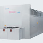
Meanwhile, TEL is significantly expanding its single wafer deposition systems. Specifically, in response to customers’ needs to advance device scaling and 3D stacking.
Particularly, the Episode 1 platform integrates up to eight process modules and supports continuous execution of multiple processes. Thus, offering customers the ability to handle increasingly complex processes as device features continue to shrink.
Moreover, the platform can be configured with the OPTCURETM module. Specifically, it removes the native oxide layer from silicon wafers and the ORTASTM module for depositing titanium, both of which help reduce the contact resistance of metal interconnects in advanced logic devices.
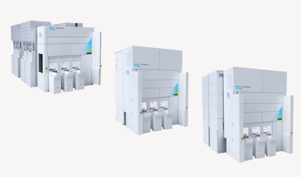
On the other hand, Episode 2 is a platform capable of simultaneously transferring two wafers. Combining high productivity and a reduced footprint, the system can significantly improve customers’ fab efficiency. Two types of process modules designed with different concepts will become available for this platform.
The DMR (Duo matched reactor) module can simultaneously perform deposition on two wafers. Succeeding the Triase+ TM EX-IITM series of products, DMR also offers various new features. Specifically, dealing with continued 3D device stacking and higher aspect ratios.
Consequently, the QMR (Quad matched reactor) module is capable of simultaneous deposition on four wafers. Thus, the module uses an innovative plasma source, supporting the plasma deposition process that has significant market growth potential.
Improves Efficiency
Unlike their predecessors, the Episode series of products come with enhanced equipment data collection and edge data processing systems. Combined with other features including an analytics application, Episode can improve equipment availability and engineer efficiency. Furthermore, the data on equipment availability and energy use are integrated in a database, which can be used to help reduce the burden on the environment.
“The Episode series has evolved from the Triase+ TM series that has been favored by our customers for many years,” says Shigeki Nakatani, Vice President & General Manager, TFF BU.
In addition, Nakatani said, “The Episode series of single wafer deposition systems can handle even more complex processes while offering high levels of productivity and environmental performance. We will continue to satisfy our customers’ needs through persistent technology development and process module enhancements.”
08 July 2024
- Share: