ASIA ELECTRONICS INDUSTRYYOUR WINDOW TO SMART MANUFACTURING
Omron to Surge in Taiwan With More Innovative Tools
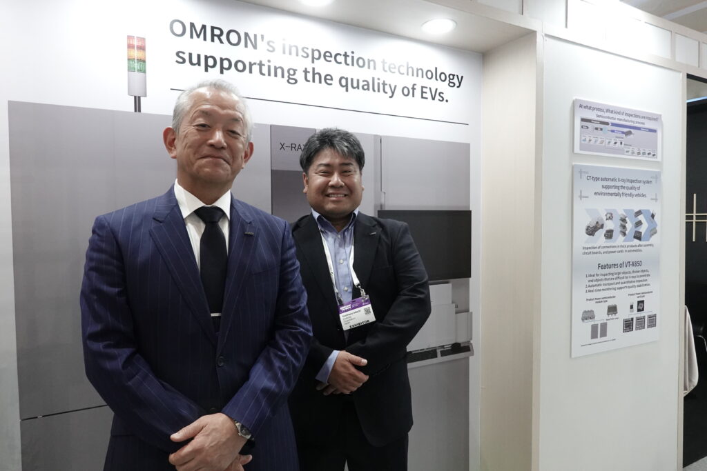
OMRON Corporation has upped the ante with its presence in Taiwan, which is a hub of advanced manufacturing and one of the major semiconductor hubs in the world. Thus, OMRON took part in the recent Semicon Taiwan 2024 and highlighted its latest innovations in semiconductor inspection.
Specifically, the company introduced its cutting-edge CT-type X-ray automatic inspection systems, VT-X850 and VT-X950.
OMRON’s Advanced Inspection Solutions
The VT-X850, which launched in February 2024, comes with a high-power X-ray source. For that reason, making it ideal for inspecting power semiconductors, IGBT modules, and inverter modules used in electric vehicles (EVs). Its capabilities address the growing demand for precise and efficient semiconductor inspection solutions.

The upcoming VT-X950, which will go on sale in March 2025, will come equipped with an ultra-microfocus X-ray source tailored for advanced packaging needs. This system can inspect smaller and more complex component. Thus, reflecting the industry’s trend toward miniaturization and integration, especially in high-performance semiconductor packages.
Addressing Chiplet Inspection Challenges
Recently, there have been strong demands for new packaging methods, such as chiplet-based architectures. Specifically, these architectures require more precision and comprehensive inspection techniques. The emergence of new application trends such as generative AI, data centers, as well as 5G/6G technologies have been driving these new packaging methods.
A key challenge with Chiplet-based designs is the ability to inspect multiple layers within a single device. These include flip chips, C4 bumps, and micro bumps used in 3D mounting. Each layer needs accurate and qualitative inspection without damaging the device.
OMRON’s VT-X950 meets this challenge. Specifically, it offers industry-leading high-speed CT imaging that captures 3D data quickly for solder form non-compliance (NG) and solder void measurement. The system leverages AI-powered automation to set inspection parameters and distinguish between good and defective parts. This advanced imaging capability visualizes the internal chiplet solder joint conditions, making it ideal for use in CPU, GPU, and communications chips.
Efficiency Gains in Semiconductor Development
Conventional inspection methods, often performed outside the production line, can take several hours to image a single location in detail. Moreover, it may take up to two to three days to analyze and compare results. The VT-X950 significantly improves this process. It can perform high-resolution imaging in as little as 18sec at a minimum resolution of 0.2µm.
In addition, the system also automatically identifies defective areas based on quantitative criteria. This dramatically reduces the time and labor required for semiconductor development. By combining the VT-X950 with existing analytical X-ray equipment, semiconductor manufacturers can optimize their inspection processes and improve overall efficiency.
OMRON’s Strategic Focus in Taiwan
In addition to showcasing its innovative technology, OMRON’s Senior General Manager of Inspection Systems Business Division HQ , Mr. Kazuhisa Shibuya, delivered a keynote speech at the Strategy Materials Conference of Semicon Taiwan 2024. He outlined how OMRON’s solutions address key concerns in semiconductor R&D and production.
“VT-X950 can be used to improve yield rates during the R&D phase, optimize production quality during initial mass production, and stabilize quality through real-time monitoring in high-volume production,” Shibuya explained.
OMRON’s broad portfolio of products and its software give the company a better position to make a significant impact in Taiwan’s semiconductor industry. The company can demonstrate the capabilities of its VT-X950 system to potential customers. Thus, helping them address their most pressing challenges in semiconductor inspection and production.
09 September 2024


