ASIA ELECTRONICS INDUSTRYYOUR WINDOW TO SMART MANUFACTURING
Defying down cycle, Lasertec capitalizes on rapid proliferation of EUV equipment
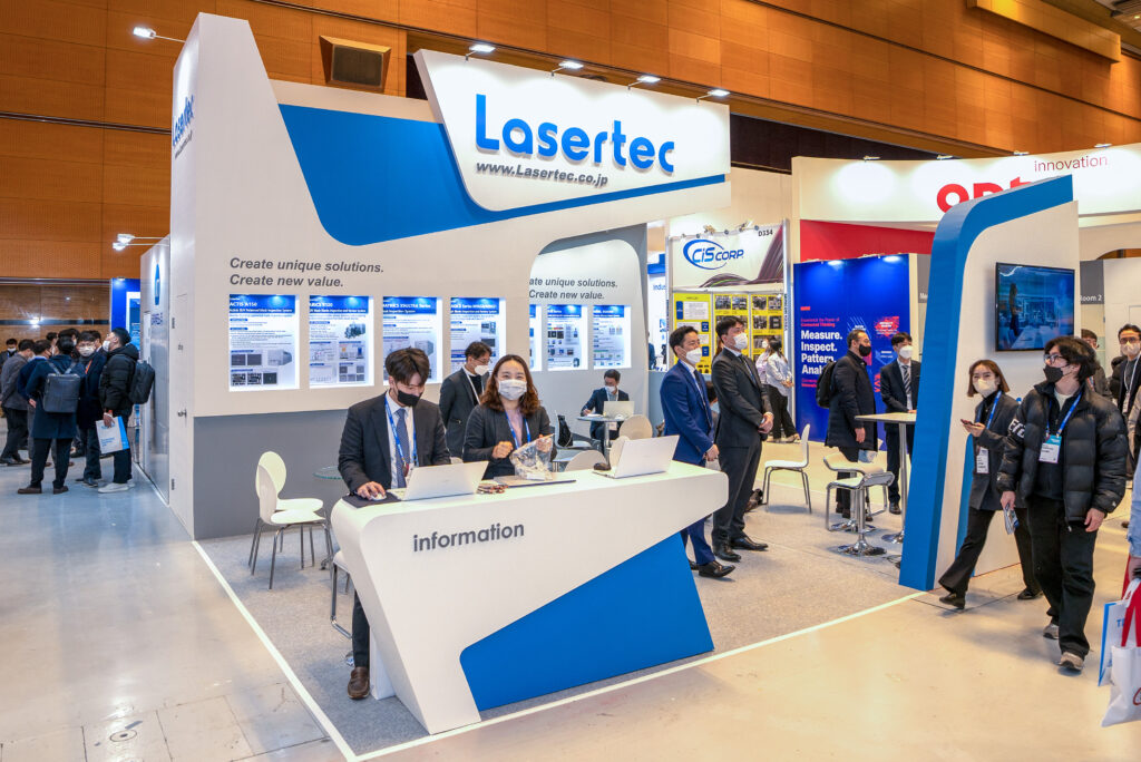
Lasertec, a Japanese semiconductor equipment maker, is consolidating its market position as a No. 1 total inspection solution provider for EUV photomask and pellicle system.
As EUV, or extreme ultraviolet lithography technology is rapidly emerging a must-have for achieving below-10nm circuitry technology, the Japanese semiconductor wafer and photomask inspection equipment maker sees huge market opportunities in the chipmaking industry’s rapid adoption of the EUV lithography ecosystem
“Even if the down cycle has begun, global market leaders like Samsung Electronics will likely continue to invest in EUV system. Accordingly, we see orders keep rolling in,” Lim Choon Gap, director of sales group with Lasertec Korea Corp.
According to him, it has been just one year after the EUV lithography equipment started mass-production. Even though the overall ecosystem for EUV mass-production lines is still premature, the adoption has been accelerating across IDMs (integrated device manufacturer) and foundry chipmakers, because the technology is one of the indispensable part of their ramp-up plan to a next generation chip processing technologies.
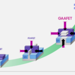
When it comes to SoCs, for example, the system is a sole technology enabler for reaching below 10n circuitry patterning. In a race to attain 3nm and 5nm circuitry technologies, IDM and foundry chip makers are aggressively adopting the new lithography technology
The same is true of memory chip makers who are struggling to ramp up to the mid to low 10s nanometer chip geometry technologies like 13 nm and 14nm.
This helps explain why chipmakers like Samsung Electronics, TSMC and Intel are making huge bet on EUV equipment and ecosystem.
Sea changes in lithography ecosystem
A short for extreme ultra-violet, the EUV system is indeed a new breed of disruptive photolithography equipment that uses rays of ultra-short wavelength EUV light as light sources to draw a chip circuitry pattern of below 10nm geometry on a silicon wafer.
As the technology is sort of disruptive technology evolution that is a dramatic break from conventional immersion or ArF light source lithography in system requirements and performances, it also calls for drastic sea changes in the overall photo lithography ecosystem, including system itself as well as peripherals like photomasks, pellicles, photo resist, and etc.
Lasertec is cashing in on the wide and rapid build-up of EUV ecosystem, as the ultra-high definition and complex chip circuitry patterning system requires a variety of inspection equipment of the same definition and complexity.
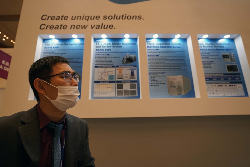
Lasertec is offering a series of inspection equipment for EUV ecosystem, including EUV blank and patterned photomask inspection equipment, EUV mask backside inspection and cleaning equipment, and EUV mask edge inspection equipment.
For example, its ACTIS A150 series of inspection system, the latest in its EUV inspection offering, is the world’s first and purely EUV-dedicated EUV patterned photomask inspection solution that uses 13.5 nm EUV light to perform actinic inspection to detect printable and phase defects on EUV masks. The actinic inspection is even able to perform through-pellicle mask inspections.
Scalable to future nodes with high NA (numerical aperture) EUV, the ACTIS series can meet performance requirements of 5nm node and beyond, enabling chipmakers to do die-to-die inspection. Soon, die-to-database inspection will available, too, as the company is now working on the enhanced version of the series.
From pellicles to masks
“The ACTIS is the world’s sole EUV patterned mask inspection system that uses the same 13.5nm wavelength EUV light source. The series are widely used across chipmakers in Taiwan, US., and Korea,” director Lim.
The company also supplies MATRICS X9 Ultra series of inspection equipment that uses 193nm laser light source to perform pellicle-less EUV mask inspection in the technology nodes of 3nm and beyond.
Also available are its MAGICS and ABICS series that are designed to inspect blank EUV photo masks. Moving down the product line-up, the company has BASIC series up its sleeve, which are designed to inspect the backside of the EUV mask, while readying inspection equipment for pellicles.
“Before drawing chip circuitry patterns on a mask, you have our MAGICS and ABICS series to inspect blank masks, and then ACTIS and MATRICS are available for pattered mask inspection. We also supply BASIC for backside inspection and MZ for mask edge inspection. In short, we finally came to become a total EUV inspection solution provider from blank and patterned masks to pellicles, director Lim stressed.
He expects that Lasertec would receive orders of EUV inspection equipment in a neighborhood of between 40 and 50 units in 2023 in Korea alone, up from the range of 30 to 40 units received in 2022.
EUV inspection equipment are usually paired with EUV lithography equipment in a ratio of 2 or 1.5 to 1, or 2 or 1.5 units for one unit of EUV lithography equipment. When it comes to ACTIS series, it will take approximately 5 hours to complete EUV patterned mask inspection.
Looking forward, Lasertec forecast that it would perform better from 2023 through 2024 in terms of sales, as the growing complexity of chipmaking processes would further stir up demand for high precision inspection system like Lasertec’s
- Share: