ASIA ELECTRONICS INDUSTRYYOUR WINDOW TO SMART MANUFACTURING
Resonac to Soar High With New SiC Line in Japan
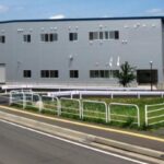
Resonac Corporation has announced the start of construction of a new production building for silicon carbide (SiC) wafers for power semiconductors. Specifically, its subsidiary, Resonac hard Disk Corporation, is supervising the construction of the new plant at its Yamagata Plant in Higashine City in Japan’s Yamagata.
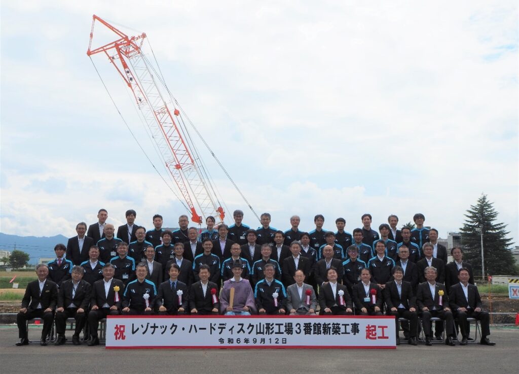
The company held a groundbreaking ceremony on September 12 that signaled the start of the construction.
Core Growth Business
This new facility is a part of Resonac’s efforts to realize the supply assurance plan for semiconductor materials (SiC wafers). Accordingly, the Ministry of Economy, Trade, and Industry, under the Economic Security Promotion Act, recognizes the importance of these specific materials.
local dignitaries including Mayor Seigo Tsuchida of Higashine City and other related parties from Yamagata Prefecture attended the groundbreaking ceremony. Meanwhile, representing the Resonac Group are Makoto Takeda, Executive Officer, General Manager of the Device Solutions Business Unit. Several other company executives participated in the ceremony.
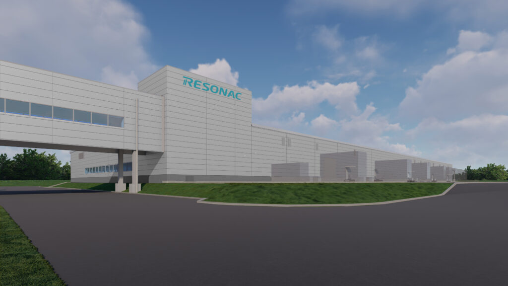
Most importantly, the company announced it expects the completion of the building in the third quarter of 2025.
As a “Co-Creative Chemical Company,” the Resonac Group aims to contribute to the sustainable development of the global society. Thus, it has positioned SiC epitaxial wafers, which support efficient use of energy, as a core growth business. The Resonac Group will continue to contribute to the proliferation of SiC power semiconductors by supplying high-performance and highly reliable products. Thus, realizing the company’s motto, which is “Best in Class”.
Background
High-end models of power semiconductors for use in high-priced EVs and railcars are required to conduct higher-density electric current. This aims to achieve high output and space saving concurrently. Thus, to realize the conduction of high-density electric current, SiC-epi-wafer manufacturers must develop a technology to prevent the expansion of dislocation defects. Specifically, those existing in SiC substrate into epitaxial SiC layer.
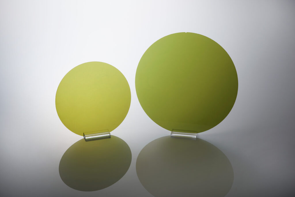
This time, Resonac developed a latest technology to grow epitaxial SiC layer and successfully solved the abovementioned problem. Moreover, it started to mass produce third-generation high-grade SiC epi-wafers. This HGE-3G features high reliability under high electric current density. Further, it will contribute to the spread of SiC-based high-end power modules.
The Resonac Group aims to be a “Co-Creative Chemical Company” and contribute to the sustainable development of global society. Under this vision, Resonac positions its operation to produce SiC epitaxial wafers, which contribute to the efficient use of energy, as a next-generation business. To this end, it will allocate much of its business resources.
In September 2022, Resonac started to ship samples of 200mm SiC epi-wafers using in-house manufactured single crystal SiC wafers.*1 In addition, Resonac has been promoting “The Project to Develop SiC Wafers Technology for Next-generation Green Power Semiconductors.”*2 Specifically, it aims to improve the quality of SiC epi-wafer further. The Resonac Group will continue contributing to the spread of SiC power semiconductors. It will maintain “Best in Class” as its motto and provide high-performance and highly reliable products.
Notes
*1. For detail, please refer to the news release, “Showa Denko Starts to Ship Samples of 200mm SiC Epi-wafers,” which was announced on September 7, 2022.
*2. For detail, please refer to the news release, “Showa Denko’s Program to Develop 8-inch SiC Wafers for Next-generation Green Power Semiconductor Selected for NEDO’s Green Innovation Fund Projects,” which was announced on May 23, 2022.
- Share: