ASIA ELECTRONICS INDUSTRYYOUR WINDOW TO SMART MANUFACTURING
ASMPT's New Laser Dicing Line Results in Better Yield
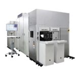
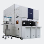
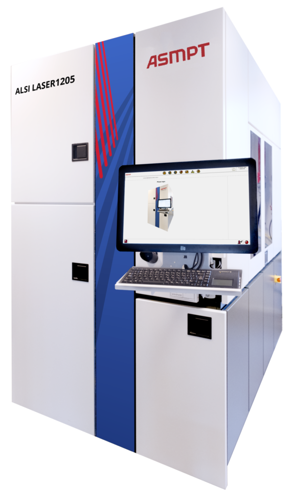
ASMPT has introduced the ALSI LASER1205, a multi-beam laser dicing platform that sets new standards in terms of precision and performance.
Accordingly, SiC is an indispensable material for the energy transition. David Felicetti, Business Development and Product Marketing Manager at ASMPT said SiC has superior electrical and thermal properties.
“Moreover, (SiC use can) produce innovative and compact power electronics for things like high-efficiency inverters. Unfortunately, SiC wafers are very thin and sensitive.”
“This has often led to low throughput and high scrap rates during dicing and grooving,” added Felicetti.
Multi-beam technology improves quality and yields
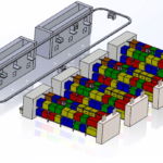
The ALSI LASER1205 multi-beam dicing platform cuts precisely, gently and efficiently. Thanks to its V-shaped patterned Diffractive Optical Element (V-DOE) developed and patented by ASMPT. The V-DOE uses multi-beam laser processes to separate semiconductor chips on a wafer. Moreover, a DOE element splits the laser beam into multiple sub-beams that simultaneously work on different areas of the wafer.
For that reason, it is possible to efficiently cut through the layers of material, which drastically speeds up the process and increases its precision.
In addition, the multi-beam technology minimizes the Heat Affected Zone (HAZ). Thus, improving the quality of the diced chips and raises their die strength to between 450 and 500 Mpa. With this proven process and continuous innovation, ASMPT has managed to increase yields significantly while maintaining high productivity.
The ALSI Laser1205 can process wafers with thicknesses ranging from 10 to 250 microns with a positioning accuracy of less than 1.5 microns. The system’s cutting width is less than 12 microns on 100 microns of silicon with the multi-beam process. All while being 50 percent faster than traditional methods.
“ASMPT has more than 20 years of experience in laser technology,” says David Felicetti. “With machines like the ALSI LASER1205, we can offer our customers the highest process quality paired with low operating costs.”
Shapes Industry Landscape
ASMPT Limited is a leading global supplier of hardware and software solutions for the manufacture of semiconductors and electronics. Accordingly, ASMPT’s offerings encompass the semiconductor assembly & packaging, and surface mount technology (SMT) industries. They range from wafer deposition to the various solutions that organize, assemble, and package delicate electronic components. Moreover, encompassing a vast range of end-user devices, which include electronics, mobile communications, computing, automotive, industrial, and LEDs.
Most importantly, ASMPT partners with customers very closely, with continuous investment in R&D helping to provide cost-effective, industry-shaping solutions. Thus, achieving higher productivity, greater reliability, and enhanced quality.
19 September 2024
