ASIA ELECTRONICS INDUSTRYYOUR WINDOW TO SMART MANUFACTURING
Resonac, Soitec to Soar Power ICs With Better Material
Resonac Corporation and Soitec have agreed to jointly develop 200mm (8-inch) silicon carbide (SiC) bonded substrates. Specifically, these substrates will serve as the material for SiC epitaxial wafers used in power semiconductors.
Soitec is a French manufacturer of advanced semiconductor substrate materials while Resonac offers an extensive lineup of semiconductor materials for back-end process.
The agreement will combine Resonac’s high-quality SiC single-crystal substrates*1 with Soitec’s substrate bonding technology. Therefore, aiming to improve the productivity of 8-inch SiC wafers and diversify the supply chain in the SiC epi-wafer business.
Improves Productivity, Reduces CO2 Emissions
Power semiconductors are gaining traction in power applications such as electrified vehicles (xEVs) and industrial equipment. Therefore, the market is likely to expand further in the future. Particularly, SiC is in high demand due to its advantages over silicon (Si). Specifically, due to its lower power loss and heat generation during power conversion. Thus, contributing to energy savings.
However, SiC single crystal substrates, which are the main material for SiC power semiconductors, require uniform crystals, advanced technology for production, and time-consuming crystal growth. For that reason, productivity improvement remains a challenge.
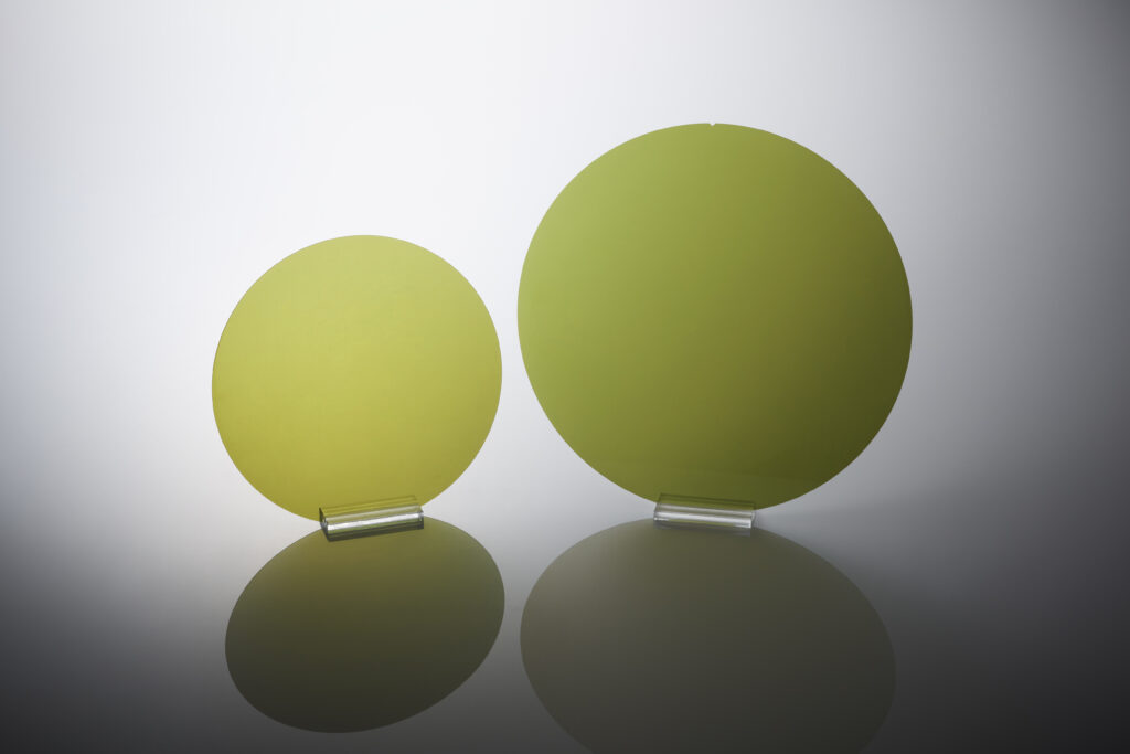
Resonac produces SiC epi-wafers with epitaxial layers grown on SiC single crystal substrates. Device manufacturers highly regard them both domestically and internationally for their world-class quality. The company is also developing 8-inch large-diameter wafers and has started shipping samples.
Meanwhile, Soitec possesses a unique technology (SmartSiC™ technology). specifically, it processes high-quality SiC single crystal substrates, bonds the processed surface to a polycrystalline SiC wafer*2 as a support substrate, and then splits the single crystal substrate into thin film. Thus, enabling the production of multiple high-quality SiC wafers from one SiC single-crystal substrate.
This technology not only improves productivity but also reduces CO2 emissions during SiC wafer manufacturing by up to 70%. Moreover, they offer environmental and cost benefits.
The bonding substrate technology has already been commercialized for Si wafers, and Soitec has expertise in its practical application.
Better Production Efficiency
In this joint development, Resonac will supply SiC single crystals to Soitec, which will then manufacture SiC-bonded substrates using these single crystals. With the collaboration, the two companies aim to improve the production efficiency of 8-inch SiC wafers. In addition, to diversify the SiC epi-wfer supply chain business.
The Resonac Group, as a “Co-creative Chemical Company,” aims to contribute to the sustainable development of the global society. Furthermore, it positions SiC epi-wafers business, which realizes efficient use of energy, as a core growth business. Moving forward, Resonac will continue contributing to the proliferation of SiC power semiconductors. Specifically, by supplying high-performance and highly reliable products under the motto of “best-in-class.”
Notes:
*1. SiC single crystal substrate: A material with a crystal structure in which atoms are arranged in a regular pattern. It has uniform physical properties and requires advanced manufacturing technology to form single crystals.
*2. Polycrystalline SiC wafer: A material composed of many small crystals (grains). Each of the small grains is a single crystal, and polycrystalline materials are aggregates of these grains. The overall crystal structure is random, making it easy to manufacture and cost-effective, and thus widely used in various applications.
26 September 2024
- Share: