ASIA ELECTRONICS INDUSTRYYOUR WINDOW TO SMART MANUFACTURING
New Keysight Wafer Test System Boosts Power IC Output
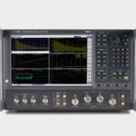
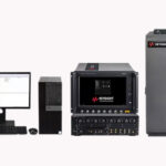
Keysight Technologies, Inc. introduces a 4881HV High Voltage Wafer Test System expanding its semiconductor test portfolio. Primarily, the solution improves the productivity of power semiconductor manufacturers by enabling parametric tests up to 3kV supporting high and low-voltage in one-pass test.
Generally, manufacturers have traditionally measured wafers using separate testers for high and low voltages. However, demand for power semiconductors is rapidly growing due to their multifunctionality, higher performance, and next-generation devices, such as silicon carbide (SiC) and gallium nitride (GaN). As a result, customers need a solution to more accurately and efficiently test their devices and reduce time to market.
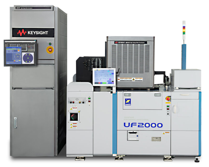
Primarily, Keysight’s solution addresses these challenges. Specifically, it allows power device makers to perform process control monitoring (PCM) and wafer acceptance testing (WAT) in manufacturing. The new test system delivers the following benefits:
High-Voltage Capability to Meet Future Needs: The high-voltage switching matrix (HV-SWM) supports up to 3kV requirements. It is scalable up to 29 pins and integrates with precision source measure units (SMUs). It enables highly flexible measurements from low current down to sub-pA resolution up to 3kV at any pins. Additionally, it supports high-voltage capacitance measurement and various parametric tests.
One-pass Testing Increases Productivity and Efficiency: The HV-SWM enables a single test system instead of separate high-voltage and low-voltage test systems. Utilizing one system is more efficient and reduces the required footprint and testing time. The system integrates with factory automation environments using Keysight’s SPECS-FA software, which improves the efficiency of the entire production process.
Enhanced Safety and Reliability: The test system has built-in protection circuitry and machine control. This ensures operators and equipment are not impacted by high-voltage surges during a test. Also, it is compliant with safety regulations, including SEMI S2 standards.
Shinji Terasawa, Vice President and General Manager of Keysight’s Wafer Test Solutions, said, “Keysight is thrilled to introduce our new wafer test system for power semiconductors, building on our long tenure of testing advanced semiconductors. Our mission is to lead the market by providing cutting-edge solutions that anticipate and meet the rapidly evolving needs of the semiconductor sector. Specifically, this latest innovation exemplifies our unwavering commitment to the industry.”
-09 October 2024-
