ASIA ELECTRONICS INDUSTRYYOUR WINDOW TO SMART MANUFACTURING
Singapore’s A*STAR to Make Way for New 200MM SiC R&D
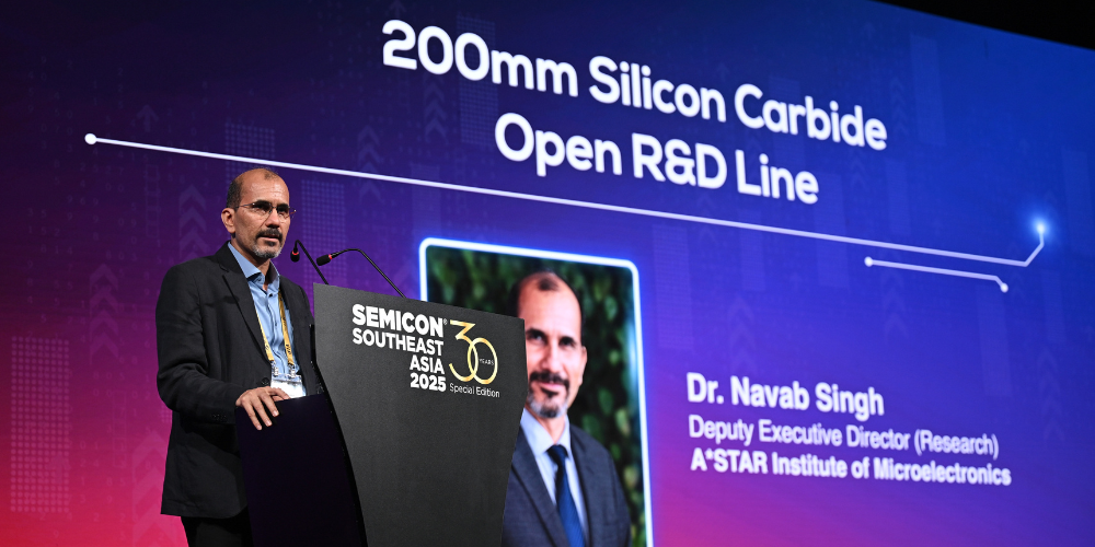
To propel and accelerate further innovation in silicon carbide (SiC), A*Star Institute of Microelectronics (A*STAR IME) of Singapore has introduced the first industry-grade 200mm SiC Open R&D Line. The said initiative will enable and accelerate SiC innovation from materials growth and defect analysist to device fabrication and testing.
The Open R&D Line aims to addresses key challenges faced in the development of SiC devices. These include high cost of industry-grade tools, limited access to advanced technologies, complex and fragmented development processes, and lack of collaboration and knowledge sharing. Moreover, the said facility will strengthen Singapore’s capabilities in wide bandgap semiconductor research and address the future demands for high-power applications.
Streamlines R&D Processes
The new facility will be offering a complete suite of SiC development and pilot manufacturing capabilities under one roof. Thus, the Open R&D Line increases the speed of R&D by eliminating the fragmented R&D processes that previously required researchers and companies to work with multiple facilities.
Furthermore, the Open R&D Line enables the development of advanced technologies by having a close partnership with key equipment OEMs and materials suppliers. Among them are ASM, centrotherm, Nissin, Soitec, and Toray, which have contributed their respective latest technologies and next-generation products.
ASM shared to A*STAR for the Open R&D Line its PE1O8 tool for depositing high-quality SiC epitaxial layers. On the other hand, centrotherm’s c.ACTIVATOR 200 and c.OXIDATOR 200 tools for high-temperature SiC annealing and oxidation.
Nissin contributed to the Open R&D Line its first and only in-situ X-ray diffraction capability for the SiC ion implantation process while Soitec has the SmartSiCTM semiconductor engineered substrate technology.
Meanwhile, Toray shared to the line its innovative materials for SiC power module packaging products.
Widens Collaboration
While it was being established, the Open R&D Line has already demonstrated its value to the semiconductor industry. Several global and local companies have partnered with A*STAR IME to utilize its capabilities. Therefore, highlighting strong industry demand for such collaborative platforms.
For one, STMicroelectronics is leveraging engineering capabilities and tools to develop ways to streamline its manufacturing processes and improve the quality of its SiC devices.
Another leading industry foundry, which A*STAR did not identify, is developing key process technologies through the Open R&D Line, with the intention to scale up production of advanced SiC devices.
Meanwhile, WaferLead, a local start-up, is using the Open R&D Line to develop, evaluate, and enhance the performance and reliability of its wafers.
27 May 2025
- Share: