ASIA ELECTRONICS INDUSTRYYOUR WINDOW TO SMART MANUFACTURING
Asahi Kasei’s New Dry Film to Meet Surge in AI Server
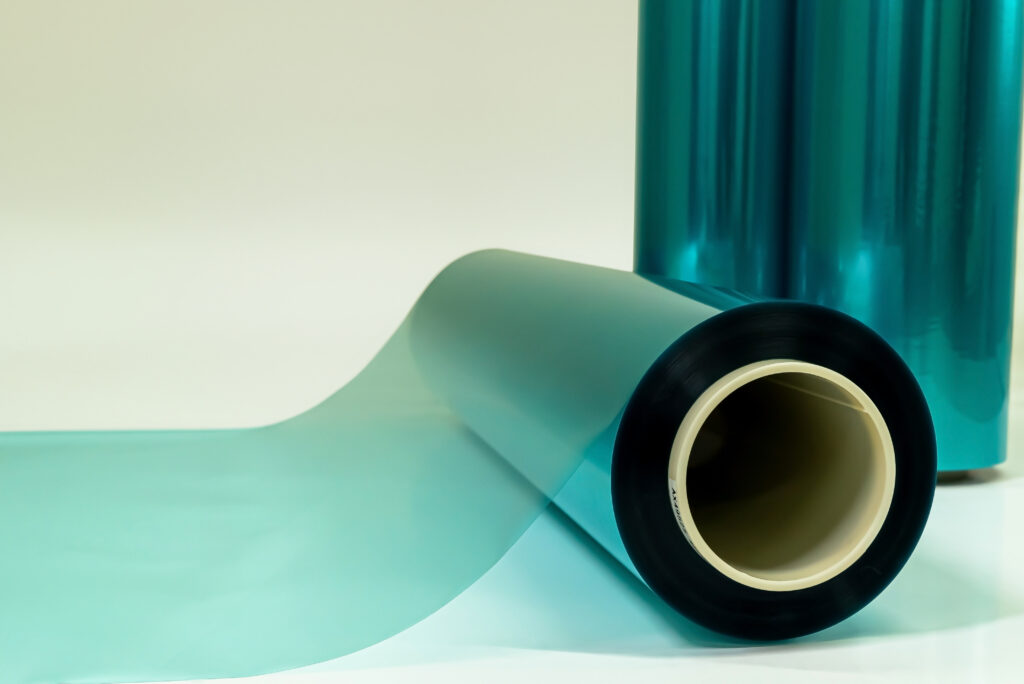
Asahi Kasei has developed the TA Series of Sunfort™ dry film photoresist as a new product designed to meet growing demand in the field of advanced semiconductor packages used in applications such as artificial intelligence (AI) servers. This product is positioned as a strategic offering within Asahi Kasei’s Material sector, aiming to strengthen its footprint in the rapidly growing market of next-generation chip packaging. The dry film delivers an ultra-high resolution with conventional stepper exposure systems and laser direct imaging (LDI) systems, which transfer circuit patterns onto substrates during packaging, contributing to enhanced performance and precision in back-end processes.
Sunfort™ dry film photoresist is a mainstay of Asahi Kasei’s Electronics business, comprising electronic materials and components. The entity is positioned as a First Priority business to drive growth under the medium-term management plan “Trailblaze Together,” with an estimated 25% increase in operating profit between fiscal 2024 and 2027 as demand for electronic components continues to expand.
Interposers serve as a bridge between chips and substrates and are used along with package substrates in advanced semiconductor packages.
These components require a large area, high-multilayer structures, and increasingly sophisticated technologies for forming high-density microwiring. In photolithography, liquid resist has long been the mainstream photoresist material for the redistribution layer (RDL) due to its superior resolution. In contrast, dry film photoresist offers advantages for panel-level processing (which involves a larger surface area than conventional wafer-level processing), such as ease of handling and ease of processing on both the top and bottom sides of the substrate. Still, it has not been adopted for RDL formation due to limited resolution performance.
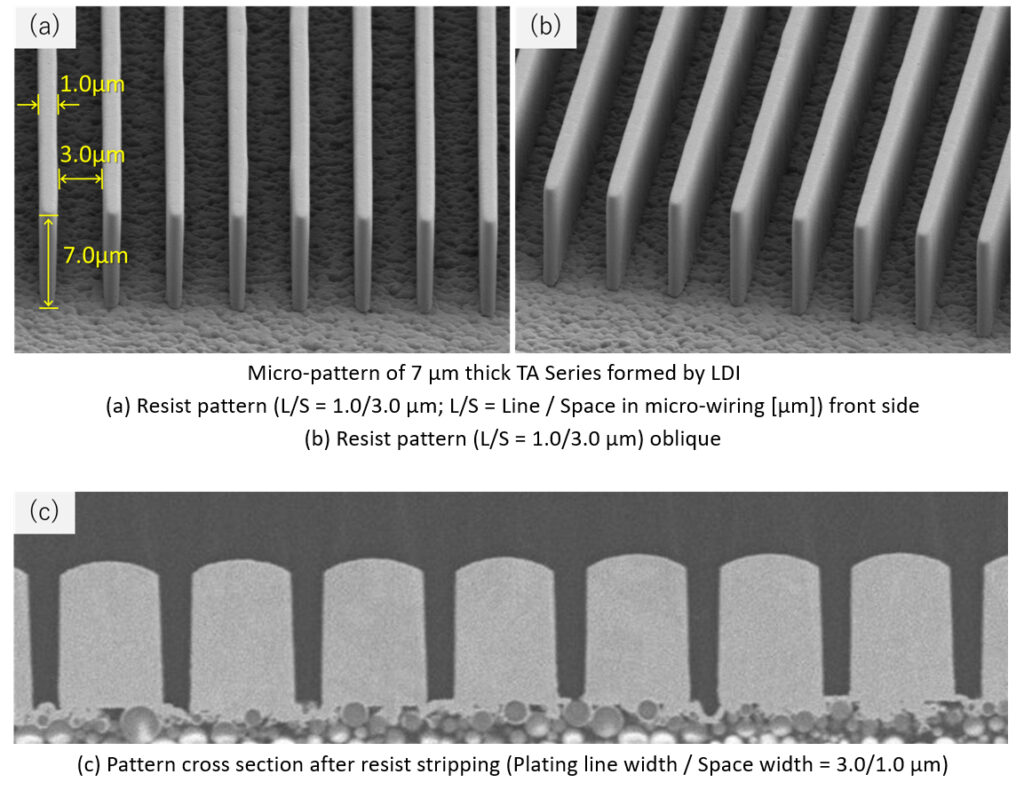
Developed based on Asahi Kasei’s long experience with photosensitive material and new material design, the TA Series enables fine wiring formation in panel-level packages and similar applications. The TA Series also allows patterning with a resist width of 1.0 µm using LDI exposure in the 4 µm pitch design required for RDL formation (see Figures a and b). The resulting fine resist pattern can be plated by a semi-additive process (SAP, a method for forming fine conductive patterns using partial electroplating), followed by resist stripping to form a 3 µm wide plating pattern in a 4 µm pitch design (Figure c).
Sunfort™ dry film photoresist will continue to play a key role in developing panel-level packaging technology as panel sizes grow. The new TA Series allows manufacturers to achieve finer wiring with greater production efficiency, helping to reduce cost and increase yield in advanced semiconductor packaging. Asahi Kasei’s TA Series comes at a pivotal time as demand in AI, automotive, and IoT markets grows.
“The development of the TA Series comes after years of close collaboration with our customers and a deep understanding of their most pressing pain points. Through this development, we address the evolving requirements of semiconductor packaging in AI, automotive, and IoT applications,” said Yu Hasegawa, Managing Executive and Senior General Manager of the Electronics Interconnecting Materials Division at Asahi Kasei. “With growing demand, particularly in Asia and North America, we at Asahi Kasei are enhancing our global support framework to deliver timely solutions and technical services tailored to regional needs.”
28 May 2025
- Share: