ASIA ELECTRONICS INDUSTRYYOUR WINDOW TO SMART MANUFACTURING
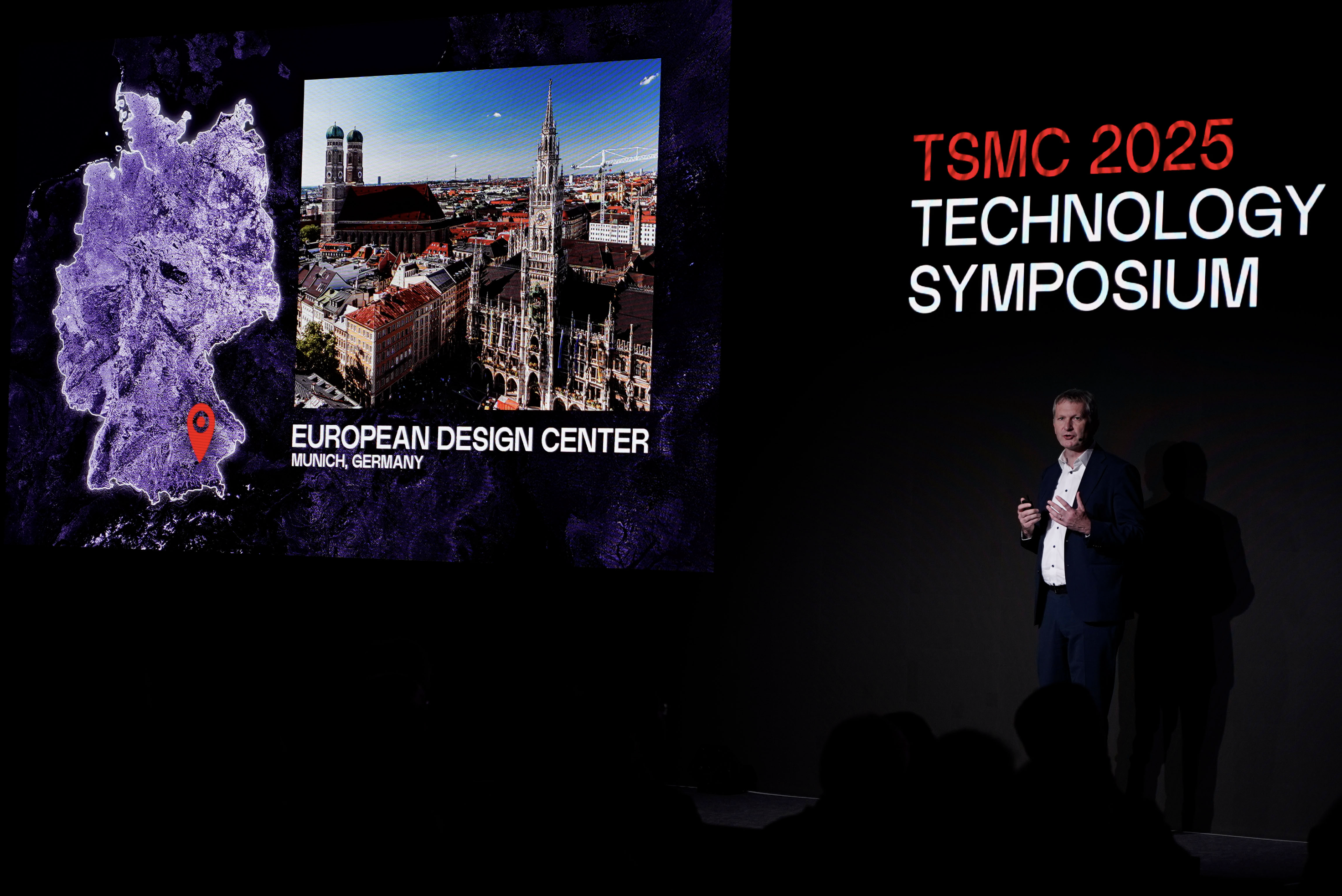
TSMC to Propel Europe Grit With New Design Center
Taiwan Semiconductor Manufacturing Company Limited (TSMC) has announced that it will establish the TSMC European Design Center (EUDC) in Munich, Germany. Accordingly, the move aims to strengthen further the company’s presence in the region.
At the TSMC 2025 Technology Symposium in Amsterdam, The Netherlands, Paul de Bot, President of TSMC Europe, said the new center will be a cornerstone to support European customers. Specifically, it will design smaller, high- performance, and energy-efficient semiconductors.
“…TSMC continues to expand its capabilities to meet customer demands and nurture innovation accross Europe,” said TSMC in its official Linkedin account, quoting de Bot.
Flexes A14 Process
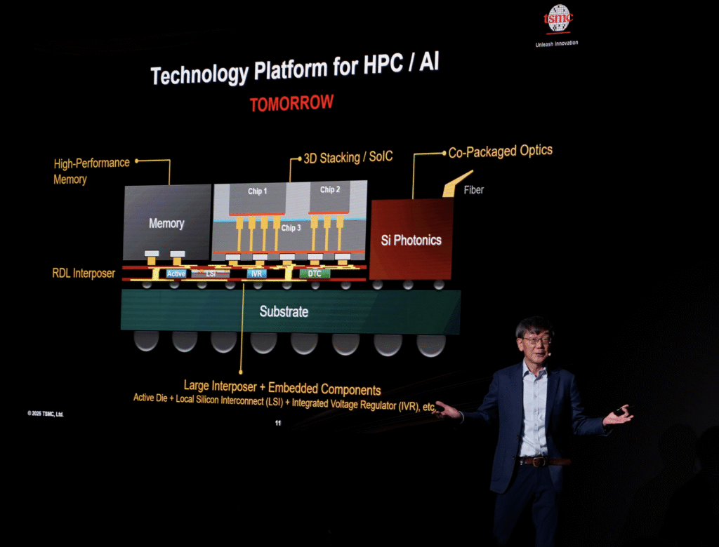
Meanwhile, Dr. Kevin Zhang, TSMC Senior Vice President of Business Development and Global Sales, also introduced at the technology symposium the A14, TSMC’s most advanced technology. A14 features NanoFlex™ Pro, an innovative and more compact cell structure that delivers unparalleled efficiency and performance.
Dr. Zhang, who is also the Deputy Co-COO, also shared the more demand for advanced technologies is seen to drive innovations forward for the automotive industry.
A14 was first announced in April at the company’s North American Technology Symposium. The 1.4nm-class technology will make significant advancements from the N2 or the 2nm-class process technology.
The A14, which the company said will enter production in 2028, will offer significant advancement from TSMC’s industry-leading N2 process. It was only in 2022 the company announced N2 process, which will go on volume production later this year (2025).
Accordingly, the company designed the new A14 class technology to drive AI transformation further as it promises to deliver faster computing and greater power efficiency.
Moreover, it will improve the on-board AI capabilities on mobile devices, making them even smarter.
Compared with the N2 process, the A14 will offer up to 15 percent speed improvement at the same power, or up to 30% power reduction at the same speed, along with more than 20% increase in logic density.
Leveraging the Company’s experience in design-technology co-optimization for nanosheet transistor, TSMC is also evolving its TSMC NanoFlex™ standard cell architecture to NanoFlex™ Pro, enabling greater performance, power efficiency and design flexibility.
ESMC JV is Right on Track
In addiiton, de Bot also the construciton of the European Semiconductor Manufacturing Company (ESMC) has been progressing well.
ESMC is a joint venture between TSMC, Bosch, Infineon, and NXP. The joint venture aims to establish an advanced semiconductor fab in Dresden, Saxony, Germany.
It marks a significant step towards supporting the future capacity needs of the fast-growing industrial, IoT, telecommunications and automotive market sectors in Europe. The fab will be of strategic importance in strengthening the European semiconductor ecosystem and unleashing innovation. Also at the event, Ray Chung, Vice President of Operations at TSMC and CEO of ESMC, shared that ESMC will first bring its leading 28/22nm planar. Eventually, it will also feature the company’s 16nm family to Europe to unleash innovations in the automotive and indsutrial sectors.
29 May 2025
- Share: