ASIA ELECTRONICS INDUSTRYYOUR WINDOW TO SMART MANUFACTURING
Apic Yamada to Surge IC Packaging With High Tech Tool
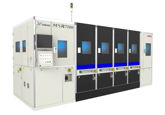
Apic Yamada Co., Ltd. has developed the MS-R series, a molding machine that is ideal for packaging a wide variety of semiconductors.
Accordingly, the MS-R Series will succeed the company’s GTM Series, which carries excellent productivity, molding precision, and versatility. Moreover, it maintains and expands its high process compatibility for a wide range of semiconductor packages, while improving production capacity and molding precision. It also incorporates our latest molding technology.
Market Background, Product Overview
In recent years, the trend toward smaller, thinner, and lower-cost semiconductor packages has accelerated at manufacturing sites. In addition, the adoption of fine packaging processes is progressing.
Accordingly, there is a simultaneous demand for higher molding accuracy than ever before, improved productivity through shorter cycle times that directly affect packaging costs, and maximizing the number of processes per shot by handling large-format, high-density boards.
In the area of power packages and modules, some of which are becoming larger and more powerful, there are expectations for process solutions that can address the following themes. First, more complex shapes, and exposed molding of terminal pin press-fit areas and installed pins. Second, exposed molding of heat sinks on one or both sides to improve heat dissipation. Next, is optimal positioning and holding of large workpieces to ensure uniform and flat resin thickness. Lastly, the ncreased resin sealing capacity.

High-performance, high-function semiconductor modules for building generative AI, which has rapidly become popular, are gaining traction in a wide range of applications. Particularly, from big data utilization servers, high-speed signal processing networking, to edge computing close to users.
In order to solve the problem of miniaturizing the semiconductor chip itself in the semiconductor front-end process, a breakthrough is necessary in the semiconductor packaging technology in the back-end process. Moreover, the evolution of semiconductor modules is becoming possible, thanks to chiplet technology, also known as 2.xD or 3D packaging process
Creation of Open Lab
Apic Yamada’s newly developed next-generation molding platform, the MS-R Series, quickly responds to these market demands and changes. Moreover, it provides new value to customers by improving productivity and molding precision, as well as realizing versatility and scalability.
In order to improve the product appeal of this series and update the development of core technologies, the company has established an open lab. Accordingly, the Apic Yamada Future Technology Laboratory, in collaboration with Nagano National College of Technology, National Institute of Technology, have begun joint research.
“We will continue to work together to improve the product appeal. This includes vibration countermeasures to accommodate high-speed operations, realization of high-precision molding technology, and labor-saving measures using AI technology,” the company said in a statement.
Product Features
- Multi-process support
It is possible to change the process between transfer molding and compression molding, and to handle general-purpose semiconductor packages that mainly use lead frames and organic substrates, as well as cutting-edge packages, all on a single platform.In
addition, by designing dedicated molds, it is also possible to handle the sintering bonding process and hybrid bonding that are increasingly being adopted for next-generation SiC power devices. - High productivity
The work handling mechanism that constitutes the equipment has been completely reviewed, a highly rigid mechanism based on vibration analysis has been adopted, and the axis control has been optimized to ensure reliability during high-speed operation, reducing waiting time loss for the press that actually performs the resin molding, and optimizing the cycle time.While
maximizing the number of processes by handling large-sized, high-density boards, the newly developed highly rigid die base unit and high-precision, high-pressure clamp die unit have ensured uniform, good molding quality across the entire area of the board. - High-precision molding
In addition to the newly developed high-rigidity mold base unit and high-precision high-pressure clamp mold unit, mold design and recipe optimization based on analysis of resin flow simulation technology have achieved molding quality that is flash-less, void-free, and has good filling properties. The above newly
developed units also enable stable process quality for MUF (mold underfill) technology, which fills resin uniformly and void-free into the narrow gaps between chips in the multi-layered chip structure used in chiplet products such as generative AI. - Automation and labor saving
The automation of workpiece transport that is supplied and collected from the magazine is realized by linking with automatic transport of OHT/AGV/AMR/HTC , etc. We are also starting to develop and consider automation functions such as automatic resin supply and waste collection.
06 December 2024


