ASIA ELECTRONICS INDUSTRYYOUR WINDOW TO SMART MANUFACTURING
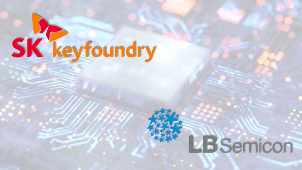
SK keyfoundry, LB Semicon Partner on New IC Packaging Tech
Korea’s 8-inch pure-play foundry SK keyfoundry has announced a collaboration with chip packaging and testing company LB Semicon. Specifically, they co-developed core technology and completed reliability testing of Direct Redistribution Layer (Direct RDL), a core semiconductor packaging technology based on 8-inch wafers.
This achievement marks a significant step forward in advancing next-generation semiconductor packaging technologies and strengthening the competitiveness of automotive semiconductor products.
Improves Connectivity, Minimizes Signal Interference
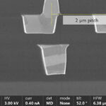
RDL refers to metal wiring and insulating layers on top of semiconductor chips to enable electrical connections. It is primarily used in Wafer Level Packaging (WLP) and Fan-Out Wafer Level Packaging (FOWLP) processes to enhance connectivity between the chip and the substrate while minimizing signal interference. In essence, the technology creates a new pattern of metal wiring and insulating layers on top of a semiconductor chip to improve connectivity and minimize signal interference.
The newly co-developed Direct RDL by SK keyfoundry and LB Semicon supports power semiconductors with high current capacity, outperforming competitors.
The technology achieves a metal wiring thickness of up to 15μm and wiring density covering up to 70 percent of the chip area.
Suits Wide Range of Applications
The intrinsic characteristics make the Direct RDL suitable not only for mobile and industrial applications but also for automotive applications.
In particular, the solution meets the Auto Grade 1 classification under AEC-Q100 international automotive semiconductor quality standard. Thus, ensuring reliable operation in harsh environments with an operating temperature range of –40℃ to +125℃.
Unlike competitors, this makes the technology fully viable for automotive products. In addition, by providing a Design Guide and Process Development Kit, SK keyfoundry can now offer a process solution tailored to customer needs, enabling smaller chip sizes, lower power consumption, and cost-effective packaging.
Stronger Foothold in Chip Packaging
LB Semicon stated that leveraging SK keyfoundry’s deep understanding of semiconductor processes and advanced manufacturing capabilities significantly shortened the development timeline. Through the integration of its own back-end processing technologies with SK keyfoundry’s foundry process expertise, the two companies have achieved optimized wafer-level Direct RDL formation, which is expected to greatly enhance production efficiency.
LB Semicon’s CEO Namseog Kim the joint development is an important milestone and LB Semicon and SK keyfoundry plan to establish a strong foothold in next-generation semiconductor packaging market.
Meanwhile, Derek D. Lee, CEO of SK keyfoundry said the integration of their respective expertise would further pave the way for high performance and highly reliable semiconductor solutions.
Headquartered in Korea, SK keyfoundry provides specialty Analog and Mixed-Signal foundry services for semiconductor companies to serve a wide range of applications in the consumer, communications, computing, automotive and industrial industries.
On the other hand, LB Semicon has been specializing in wafer bumping, redistribution services, wafer probing, and die processing since 2000. Moreover, they also in various packaging solutions like wafer-level packaging and chip-on-film packaging. They are a key manufacturing partner for major semiconductor firms, foundries, and electronics companies globally.
27 July 2025
- Share: