ASIA ELECTRONICS INDUSTRYYOUR WINDOW TO SMART MANUFACTURING
Advantest’s New CD-SEM to Meet Needs of 2nm and Beyond
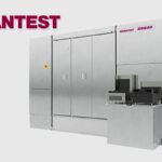
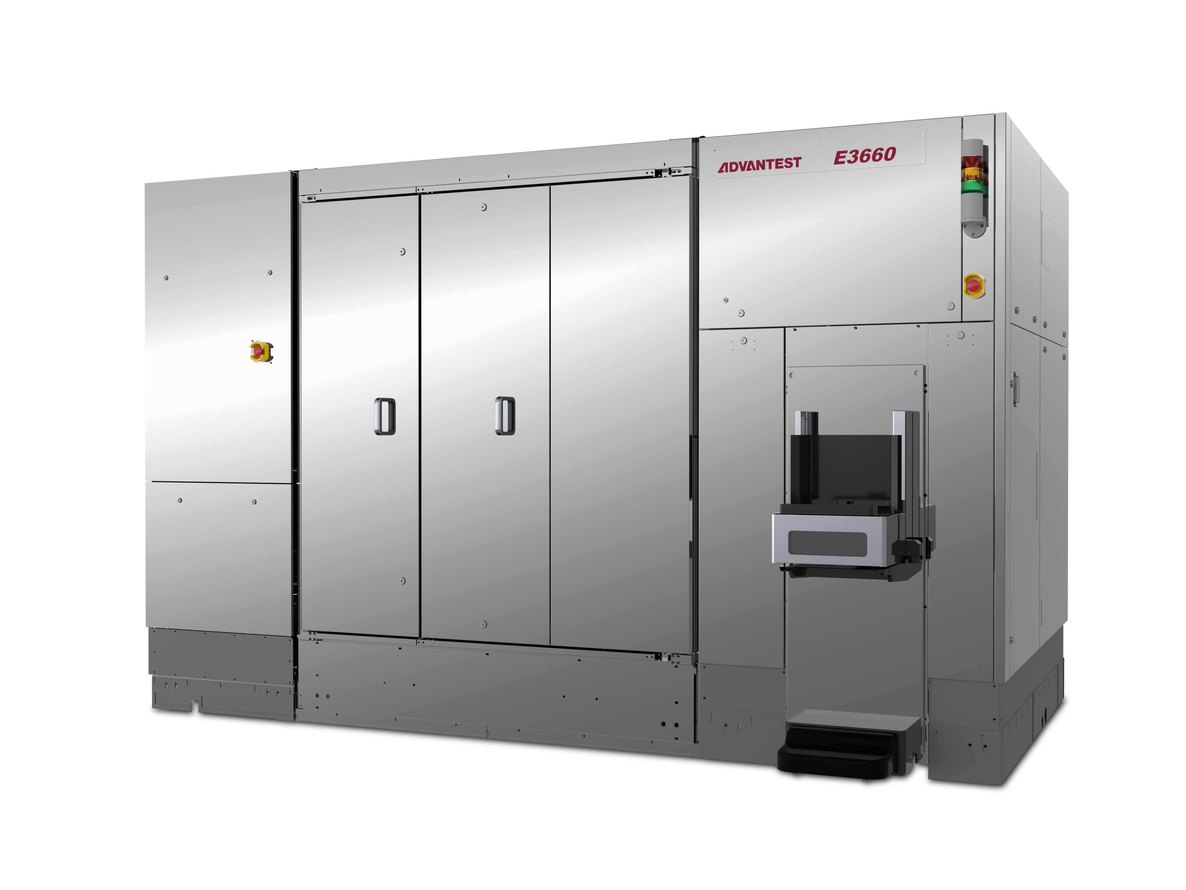
Leading semiconductor test equipment supplier Advantest Corporation has introduced its next-generation E3660 Critical Dimension Scanning Electron Microscope (CD-SEM). Specifically, it is engineered for the dimensional metrology of photomasks and EUV masks used in cutting-edge semiconductor manufacturing.
Advantest’s E3660 delivers more than a 20 percent improvement in CD reproducibility. Therefore, enabling process engineers to meet the stringent requirements of mask manufacturing at the 2nm node and beyond. By reinforcing lithography process control in advanced device fabrication, the E3660 furthers Advantest’s vision of providing holistic test solutions across the semiconductor value chain.
Guarantees Desing-to-Mask Fidelity
Advanced semiconductor device fabrication requires continuous scaling and pattern complexity. Therefore, this drives a sharp increase in lithographic hotspots, where multi-patterning and pattern transfer become particularly error-prone. Specifically, masks used to form wafer circuitry are evolving, with higher layer counts and more intricate geometries. This, in turn, has significantly increased the number of required metrology sites, demanding measurement systems with both higher throughput and superior reproducibility.
Moreover, the industry is also transitioning toward curvilinear mask patterns, enabled by advances in multi-beam mask writing and high-performance computing. These patterns are likely to see large-scale deployment around 2027 with the adoption of High Numerical Aperture EUV lithography in device production.
Design-to-mask fidelity under the above conditions is necessary. Therefore, CD-SEMs must not only provide highly reproducible critical dimension measurements but also generate SEM images with greater fidelity to true pattern contours. In addition, metrology solutions must evolve to incorporate curvature-sensitive algorithms capable of quantifying deviations between complex mask features and original design intent.
Partnership With imec
Leading up to the development of the E3660, Advantest has collaborated with imec, a research and innovation, to validate the correlation of CD-SEM results obtained from the E3650 with those from Advantest’s previous generation CD-SEMs and EDA-based reference data.
This enabled Advantest to improve metrology reliability and work with imec to advance the development and validation of new measurement techniques for curvilinear geometries. The E3660 platform reflects the outcome of this collaboration, achieving the reproducibility required for 2nm node mask manufacturing. Therefore, enabling high-throughput measurement to handle increasing site counts, and providing unique measurement functions for curvilinear patterns.
By integrating these capabilities, the E3660 is positioned to deliver robust metrology support for the next generation of mask R&D and production environments.
10 September 2025
- Share: