ASIA ELECTRONICS INDUSTRYYOUR WINDOW TO SMART MANUFACTURING
Samsung Joins Applied’s EPIC Center, to Soar Chip R&D
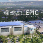
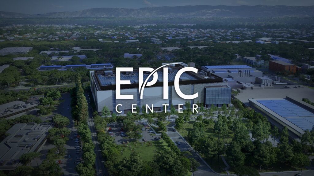
Applied Materials said Korean conglomerate Samsung Electronics will join the new US$5 billion EPIC Center, which will open in Silicon Valley this year. Accordingly, Applied’s EPIC Center will be the world’s largest and most advanced facility for collaborative semiconductor process technology and manufacturing equipment R&D.
Gary Dickerson, President and CEO of Applied Materials said the global buildout of AI infrastructure is driving unprecedented demand for energy-efficient chips. That said, Dickerson said “Our industry must rethink and re-engineer how we collaborate to deliver the next generation of manufacturing technologies. Samsung will join Applied Materials at the EPIC Center, where our teams will work side-by-side to accelerate the path to bring advanced technologies to market faster than ever before.”
Meanwhile, Young Hyun Jun, Vice Chairman and CEO of Samsung Electronics said the two companies continue to build on long-standing partnership to advance leading-edge semiconductor.
Accelerates Chip Roadmap
Applied Materials first announced its investment to Equipment and Process Innovation and Commercialization (EPIC) Center in 2023. Specifically, it is designed to accelerate development and commercialization of the foundational technologies needed by the global semiconductor and computing industries.
A traditional chip development cycle is a serial compartmentalized process that can take 10 to 15 years, but the EPIC model and infrastructure will drastically reduce that time, enabling parallel development, agile handoffs and early access to next-generation processes across the ecosystem.
The co-development programs at the EPIC Center aims to fast-track the development and deployment of next-generation semiconductor technologies through high-velocity co-innovation. The joint R&D programs will target new materials and process technologies for chips multiple nodes ahead of the current generation. Moreover, it will also target new atomic-scale innovations for advanced patterning, etch and deposition processes to enable new generation of devices across advanced logic and memory chips.
According to Applied Materials, the EPIC Center represents the largest-ever U.S. investment in advanced semiconductor equipment R&D.
With more than 180,000 square feet of state‑of‑the‑art cleanroom space for collaborative R&D, the facility is on track to become operational in spring 2026.
12 February 2026
- Share: