ASIA ELECTRONICS INDUSTRYYOUR WINDOW TO SMART MANUFACTURING
TSMC Reveals New A13, A12 Process Tech as AI Chips
Taiwanese chipmaker TSMC announced Wednesday (Apr. 23, Tokyo) the latest innovation A13 process chip, its most advanced process technology to date. The cutting-edge chip will pave the way for an even more compact and efficient designs to address insatiable compute demand for next-generation artificial intelligence, high performance computing (HPC), and mobile applications.
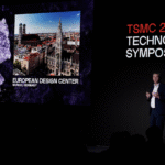
The new A13, announced at the company’s 2026 North America Technology Symposium in Santa Clara, California, is a direct shrink of its industry-leading A14 it introduced in the same event last year.
Moreover, the company also provided a sneak peek of another up-and-coming chip node, the A12, an A14 platform enhancement and features the Super Power Rail technology to provide backside power delivery for AI and HPC applications. TSMC said production of A12 will happen in 2029.
A13 was one of many technology innovations highlighted at TSMC’s North America Technology Symposium, which kicks off the event series around the world in the coming months. With the theme of “Expanding AI with Leadership Silicon,” the technology symposiums are TSMC’s largest annual customer events, showcasing the Company’s breakthroughs in technology development and manufacturing service.

Lead in Industry Density, Performance
TSMC’s A13 will offer 6 percent area savings from A14 but will still manage to deliver increased power efficiency and performance gains through design technology co-optimization.
The A13, which is backward-compatible with its A14 predecessor, is scheduled to enter production in 2029, one year after A14.
TSMC Chairman and CEO Dr. C.C. Wei said the new A13 is meticulously engineered to be ready for high-volume production just right in time when new designs demand them.
“TSMC’s advanced process technologies lead the industry in density, performance and power efficiency, and we continually strive to make them even better for our customers’ future products, ensuring customers’ success as their most reliable technological partner,” said Wei.
Other Technologies
TSMC’s North America Technology Symposium also unveiled other key technologies.
In the area of packaging and stacking, TSMC said it will continue to expand its Chip on Wafer on Substrate (CoWoS) technology to integrate more silicon. Specifically, the company is now producing 5.5-reticle size CoWoS andplanning for even larger versions. A 14-reticle size CoWoS, slated for 2028 production, can be capable of integrating approximately 10 large compute dies and 20 HBM stacks. This will be followed by an expansion to beyond 14 reticles in 2029.
TSMC is also offering its TSMC-SoIC 3D chip stacking technology on its most advanced technology platform with A14-to-A14 SoIC scheduled for production in 2029. It will support higher bandwidth of data transfer betweek stacked chips as it will provide 1.8x higher di-to-die I/O density compared with N2-on-N2 SOIC.
TSMC will also begin production towards 2026 of its Compact Universal Photonic Engine (TSMC-COUPE), which is set to reach a milestone with a true- co-packaged optics solution using COUPE on substrate. The integrated COUPE optical engine directly inside the package will enable TSMC to achieve 2x power efficiency and 10x latency reduction versus a pluggable version on the circuit board.
TSMC also announced its new N2A, its first automotive-grade process technology with nanosheet transistors that will meet demanding requirements of advanced driver assistance systems (ADAS) and autonomous vehicles as well as other physical AI applications such as humanoid robots.
Meanwhile, TSMC also announced that its N3A automotive process technology will enter production in 2026.
23 April 2026
- Share: