


ASIA ELECTRONICS INDUSTRYYOUR WINDOW TO SMART MANUFACTURING
Imec, EVG Push High Yield 200nm Hybrid Bonding
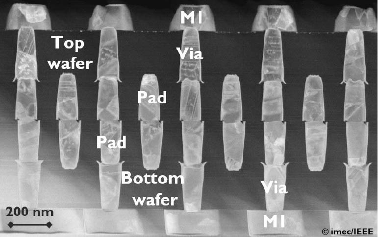
imec and EV Group (EVG) have unveiled a high-performance wafer-to-wafer hybrid bonding technology at a 200nm copper (Cu) interconnect pad pitch. The solution, demonstrated on a test vehicle with routable interconnects, targets next-generation 3D semiconductor architectures requiring extremely dense interconnects.
The joint achievement, featured at the 2026 IEEE Electronic Components and Technology Conference (ECTC), also delivered record Cu pad alignment accuracy using EVG’s advanced wafer bonding equipment. The companies said the milestone supports future scaling needs for logic-to-logic and memory-to-logic stacking in advanced system designs.
Record Overlay Accuracy Across 300mm Wafer
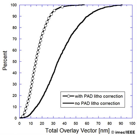
Imec reported a Cu pad-to-pad post-bond overlay below 40nm across 100 percent of dies on a full 300mm wafer, which it described as a world first. The result was achieved using wafers pre-processed with four layers of routable interconnects prior to bonding.
EVG’s GEMINI FB hybrid and fusion bonding system played a central role in reaching this level of precision. The overlay accuracy is critical for ensuring high electrical yield in advanced semiconductor manufacturing.
CMOS 2.0 Drives Demand for High-Density Interconnects
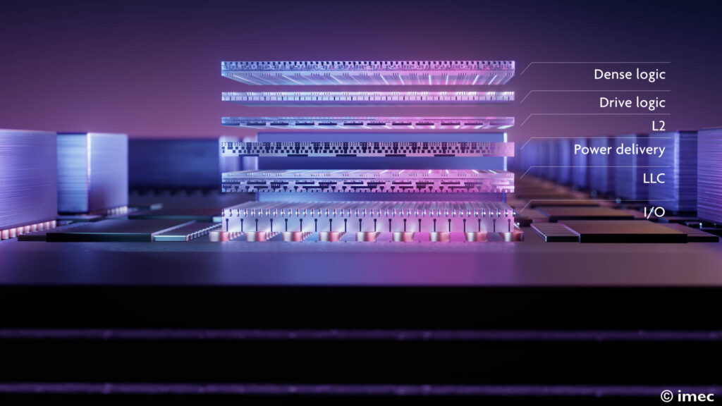
The breakthrough aligns with imec’s CMOS 2.0 scaling paradigm, which restructures system-on-chip (SoC) architectures into heterogeneous functional tiers connected through 3D interconnect technologies.
In this framework, logic components can be divided into high-drive and high-density layers, requiring ultra-dense interconnects to maintain performance. Wafer-to-wafer hybrid bonding is positioned as a key enabler of this approach.
Process Optimization Enables Breakthrough
According to imec, the results were achieved by co-optimizing critical elements of the hybrid bonding process flow. These include the use of silicon carbon nitride (SiCN) as the dielectric material and a chemical mechanical polishing (CMP) step designed to deliver uniform dielectric surfaces.
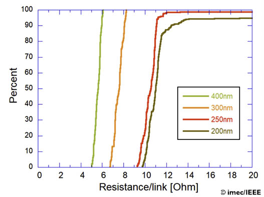
Additional factors such as improved Cu pad design and pre-bond lithography corrections contributed to the high overlay control and alignment precision.
Collaboration Targets Sub-200nm Roadmap
The partners plan to extend development beyond the 200nm interconnect pitch milestone to address future high-performance computing requirements. Further improvements in overlay accuracy will be critical as interconnect density continues to increase.
The long-running collaboration between imec and EVG continues to focus on advancing wafer bonding technologies to support emerging semiconductor device architectures and strengthen innovation across the industry.
29 May 2026
- Share: