


ASIA ELECTRONICS INDUSTRYYOUR WINDOW TO SMART MANUFACTURING
Applied to Boost EPIC Hub With SCREEN as New Partner
Applied Materials has expanded its EPIC Center collaboration network by onboarding SCREEN Semiconductor Solutions Co., Ltd. (SCREEN SPE) as a new innovation partner. The partnership will combine SCREEN SPE’s wafer cleaning expertise with Applied Materials’ materials engineering capabilities to develop co-optimized semiconductor process solutions for advanced chip manufacturing.
Addressing Rising Complexity in Chip Manufacturing
As semiconductor devices become more complex, maintaining ultra-clean wafer surfaces has emerged as a critical factor in ensuring yield, performance, and reliability at advanced process nodes. Defects introduced during deposition, etch, and materials modification must be managed with increasing precision, elevating the importance of tightly integrated cleaning processes.
By aligning technologies, Applied Materials and SCREEN SPE aim to deliver co-optimized, end-to-end solutions. The collaboration integrates Applied’s process expertise across deposition, dry etch, and materials modification with SCREEN SPE’s strengths in cleaning, wet etch, and surface preparation. The goal is to help chipmakers accelerate time-to-production while achieving higher device yields.
Expanding Collaboration at the EPIC Center
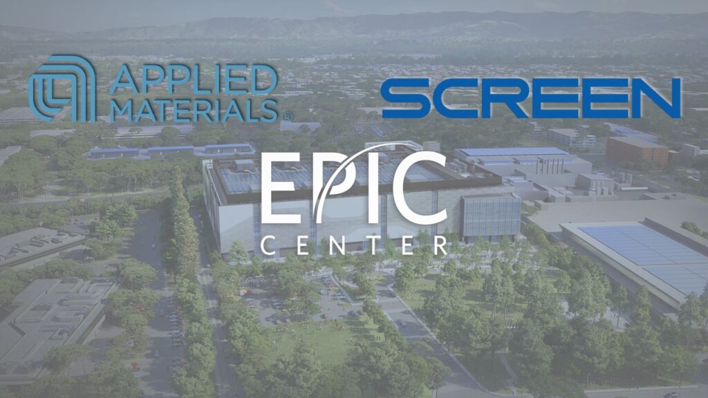
The EPIC (Equipment and Process Innovation and Commercialization) Center in Silicon Valley serves as a hub for collaborative semiconductor innovation. Designed to accelerate commercialization of next-generation technologies, the facility co-locates chipmakers, equipment providers, and research teams to streamline development cycles.
According to Dr. Prabu Raja, President of Applied Materials’ Semiconductor Products Group, integrating SCREEN SPE’s technologies enhances the ability to address complex surface engineering challenges. By combining capabilities at the EPIC Center, the companies can develop process solutions more efficiently as customers push toward new technology frontiers.
SCREEN SPE President Akihiko Okamoto emphasized that as device structures grow more intricate, the interface between cleaning, wet etch, and other process steps becomes increasingly critical. The EPIC Center enables evaluation of optimized solutions across full process flows, supporting higher performance and reliability for advanced devices.
Building on Existing Technical Collaboration
The partnership builds on an established relationship between the two companies, including joint process development at Applied Materials’ META (Materials Engineering Technology Accelerator) Center in Albany, New York. SCREEN SPE’s single-wafer cleaning systems have been used there to support cleaning optimization across film formation, etch, and ion implantation processes.
The EPIC collaboration significantly extends this work, allowing engineering teams to operate in closer proximity and tackle a broader range of process challenges. This setup enables faster learning cycles and tighter integration into Applied Materials’ research and development programs.
Scaling Semiconductor Innovation
Spanning more than 180,000 square feet, the EPIC Center represents Applied Materials’ largest U.S. investment in semiconductor equipment R&D. The facility is designed to reduce the time required to commercialize new technologies by as much as half, bridging early-stage research to full-scale manufacturing.
Scheduled to become operational in 2026, the EPIC Center is positioned as a central platform for advancing next-generation semiconductor technologies through collaborative innovation.
27 May 2026
- Share: