ASIA ELECTRONICS INDUSTRYYOUR WINDOW TO SMART MANUFACTURING
OMRON's New System Achieves Fast X-Ray Inspection
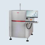
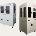
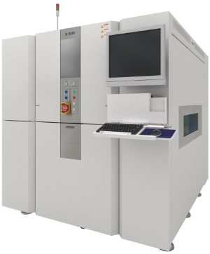
OMRON Corporation has developed the new VT-X750-V3 system, one of the industry’s fastest (*1) CT-type X-ray inspection device (*2) to date. The company released the machine to the market on November 20.
The VT-X750-V3 delivers advanced, true three-dimensional (3D) inspection of electronic substrates to meet the growing needs for 5G applications, electric vehicles (EVs), and autonomous driving systems. OMRON fosters high-speed, constraint-free printed circuit board (PCB) design, and pure X-ray inspection of electronic substrate assemblies. As such, these maintain and improve productivity while simultaneously ensuring the quality of customer products.
Total Solution, Zero Defects
In recent years, demand for electronic substrates to support 5G, EVs, and autonomous driving applications has grown rapidly. Because of this, the need to raise the quality requirements of these substrates also increased.
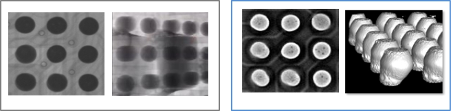
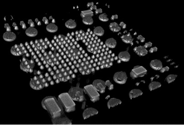
Design, manufacturing, and inspection challenges are growing such as progressing PCBA densification through IC chipping. This relates to parts mounting on both sides of the board and further consolidation of parts to increase the number of components mounted on the board. To inspect these components with true accuracy and stability, traditional 2D X-ray imaging techniques are insufficient and 3D inspection has become essential.
However, 3D X-ray imaging, image processing and inspection take time. It is very difficult to achieve both operating effectiveness and high-quality inspection. Historically, to keep pace with antiquated 2D X-ray cycle-times or meet production demands, 3D CT inspection is essential on a portion of the assembly, for the most critical components, or in an offline inspection cell away from the production line to meet 100 percent inspection requirements.
The VT-X750-V3 delivers an inspection speed 1.5 times faster than the current model, making 100 percent CT X-ray inspection of even complex substrates more achievable than ever. High-speed acquisition of clear 3D images is possible with unique, continuous imaging technology (*3) and seamless, smooth, motion through OMRON’s own machine control equipment and a camera with two times (*4) the sensitivity of conventional technology.
This allows for high performance inspection within a shorter cycle time. In addition, the CT imaging condition settings used for inspection are more automated through ongoing OMRON AI development to further reduce program tuning time. OMRON’s expertise, experience and continuous innovation have been helping to improve customer productivity for more than 30 years.
OMRON’s strategic concept of innovative-Automation consists of the three i’s: integrated (the evolution of control), intelligent (intelligence developed through IoT and AI), and interactive (new harmonization between humans and machines). Without a doubt, OMRON is driving innovations on the production floor.
By combining the integration of the widest range of control devices and the use of AI fully versed in solder inspection, the VT-X750-V3 is the latest offering from OMRON that embodies the innovative-Automation concept. Omron offers total solutions designed to achieve zero defect production lines.
Key Features
Faster inspection speeds
OMRON continues to maintain high quality imaging of 3D CT data (3D images) alongside optimized hardware control to realize inspection times 1.5 faster than the current model. This enables high-precision, 100 percent inspection without any compromise to productivity. To develop the advanced optimization of hardware control, OMRON concentrated in-house knowledge and expertise alongside OMRON motion control devices to actualize high-speed, seamless, continuous imaging and more accurate positioning with real-time feedback control.
Through these unique and innovative technologies OMRON can deliver clear 3D CT images. Additionally, the high-speed, high-sensitivity camera combined with OMRON’s latest 3D algorithms reduce X-ray noise to improve overall automated inspection capability and stability even further.
Power device inspection
OMRON has introduced new inspection logic to optimize inspection for components such as IGBT and MOSFET (*5) power devices. OMRON VT-X series 3D CT X-ray continues to be heavily utilized for solder filling inspection of through-hole connectors, inspection of press-fit connectors and inspection of SiP/PoP packages (*6), which have seen a continual increase in utilization over recent years.
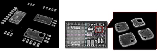
Inspection of power devices is becoming more critical as power semiconductors are changing from Si to SIC or GaN (*7) and heat release issues are becoming more important. When facing growing EV challenges and demands for increasing mileage per charge, higher power and reductions in size and weight, heat release issues are unavoidable. OMRON has developed advanced and proprietary inspection algorithms to target the critical void inspection of solder joints to help address heat release issues.
Improves automation, reduces skill level requirements
X-ray inspection frequently requires optimization of imaging conditions due to various test objects, component types or component locations on both sides of the PCB. Multiple parameters are necessary when setting these conditions. The conventional method was frequent and manual setting through trial and error until the system identifies the optimal imaging condition. However, it is now possible to automatically make these determinations with AI to significantly shorten the tuning process.
3D CT data, captured with the VT-X750-V3, need advanced and powerful technology to process 3D images. By registering the 3D image processing settings beforehand, the VT-X750-V3 can achieve true, automated inspection at the production site. However, the tuning of these settings may require specialized skills. New AI tools are helping to automate some of these processes. Thus, reducing both the setting time and necessary skill level.
Reducing the risk of X-ray exposure
In addition to preventing X-ray exposure to operators, reducing risk of failure due to over-exposure of semiconductor components subject of inspection is a real concern.
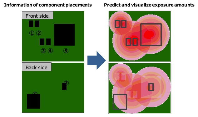
OMRON has developed a feature that can accurately simulate the exposure level per component, in any location and on both sides of the board. This new function reduces the risk of component failure due to excessive X-ray exposure by verifying dosage amounts.
References:
(*1) The world’s fastest: As a full 3D CT-type X-ray automated inspection system, it is the world’s fastest in the substrate inspection industry, according to OMRON’s research as of October 2021.
(*2) CT (computed tomography)-type X-ray automatic inspection device: Inspection device equipped with technology to capture computed processing data of 3 dimensional images when capturing the image of continuous cross-sections inside of structures that are invisible to the human eye using X-rays. The same technology as CT scanning systems utilized by medical institutions.
(*3) Continuous imaging technology: Technology for imaging stereoscopic images without stopping.
(*4) Twice as much as before when comparing the detection range of the conventional model and, in the same imaging condition, the degree to which an image sensor (imaging element) detects X-ray as light.
(*5) IGBT and MOSFET: Power devices are components that are necessary to drive motors and convert DC electricity from a battery or other sources into the AC needed by the drive motors. In recent years, it has become one of the more important components for electrification of automobiles and railways. In household electrical appliances, electricity from outlets can be used as-is to drive motors; but in automobile or PHEV applications, batteries are used as the driving source, and it is necessary to convert from DC to AC. IGBT or MOSFET are a typical power devices utilized and adopted differently depending on the application.
(*6) SiP/PoP package: SiP = System in Package, PoP = Package on Package. Both are the names of components used on sophisticated PCB designs. The Existing IC/LSI component’s inner structure is a single layer; but the SiP or PoP component inner structure is multi-layered and consists of more complicated structures. The more complex the structure, the more critical 3D X-ray inspection capabilities and high-quality imaging becomes. SiP devices are frequently used for 5G communication components such as connected cars and smartphone devices while PoP devices are frequently used for processor applications like primary CPUs.
(*7) SiC or GaN: Conventional semiconductor devices are mainly made of Si (silicone) including power devices; but many such power devices may experience heat issues as electrical voltage and current increases. SiC (Silicone carbide) or GaN (Gallium Nitride) devices have stronger heat resistance and are expected to dominate next-generation power semiconductor device designs.
- Share: