ASIA ELECTRONICS INDUSTRYYOUR WINDOW TO SMART MANUFACTURING
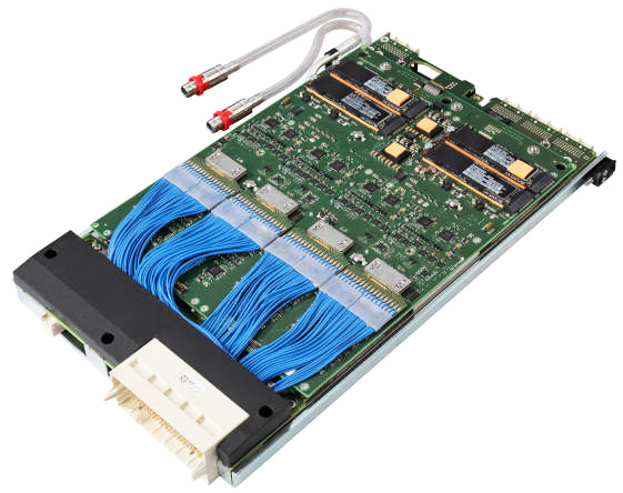
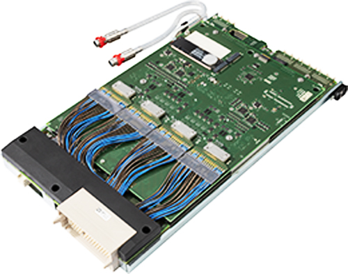
Advantest Beefs up Digital Channel Card Family
Leading semiconductor test equipment supplier Advantest Corporation has released new members of the Link Scale family of digital channel cards for the V93000 platform. The new cards enable software-based functional testing and USB/PCI Express (PCIe) SCAN testing of advanced semiconductors. They address testing challenges that require these interfaces to run in full protocol mode, adding system-like test capabilities to V93000.
Need for Ultrafast Test Transfer
Many of complex system-on-chip (SoC) devices, microprocessors, graphics processors, and artificial intelligence (AI) accelerators incorporate high-speed digital interfaces, like USB or PCIe. The new Link Scale cards use these interfaces for very fast transfer of functional and scan test content. This process increases test coverage and throughput simultaneously. Using the same form factor as all other V93000 cards, they fully integrate into the test head.
“By using a high-speed link, supporting custom operating systems and drivers, integrating local processing power and incorporating support from Advantest’s EDA partners, our Link Scale cards deliver testing and debugging capabilities that are unmatched by traditional ATE,” said Juergen Serrer, managing executive officer responsible for Advantest’s V93000 Business Unit. “This product family extends the application range of our V93000 platform into new areas, substantially enriching digital testing on ATE.”
Increase Test Quality, Shorten Time to Market
The new Link Scale cards communicate with the device under test through a standard high-speed serial interface. This allows users to test the device in its normal mode of operation using similar firmware and drivers as in the target application. The high throughput of this approach keeps the test time under control. Meanwhile, the additional functional coverage meets the stringent quality requirements of complex devices manufactured in the latest process nodes. Link Scale cards enable the use of state-of-the-art debug tools (e.g., Lauterbach TRACE32®), improving the process for first silicon bring-up and accelerating the ramp into full production.
Real-World Application Test
Pre-silicon functional tests can now be re-used, leveraging the Portable Test and Stimulus Standard (PSS). Major electronic design automation (EDA) tools support this process, which significantly increases test quality and shortens time to market. The new cards also provide a customizable environment for host software to run on the cards. It allows real-world application testing with a full software stack to be performed on the V93000 system. This facilitates the exchange of test data among different environments, such as wafer sort, final test and system-level test. As a result, the Link Scale test solution can help users establish known-good-die (KGD) strategies for chiplets in 2.5D or 3D multi-die packages.
“The collaboration between Advantest and Cadence lets customers reuse software-driven functional stress tests from design validation in high-volume manufacturing with the Cadence Perspec System Verifier,” said Yogesh Goel, vice president of business and customer development in the System & Verification Group at Cadence. “Customers can benefit from use of a widely established tool chain to automatically generate and debug tests with high coverage and short execution times.”
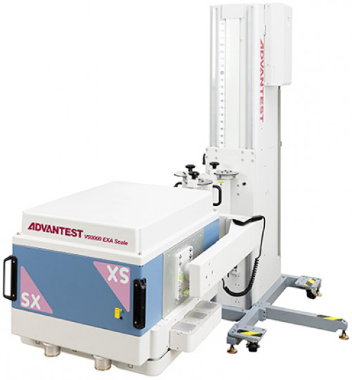
The new cards can be added to any V93000 Smart Scale or V93000 EXA Scale System. They have been delivered to pilot customers for test program development in advance of device ramp for high-volume manufacturing. They will be broadly available in the first quarter of 2022.
- Share: