ASIA ELECTRONICS INDUSTRYYOUR WINDOW TO SMART MANUFACTURING
Samsung Foundry Brings Out New Design Ecosystem for 4nm, 3nm Chips
The foundry business of Samsung Electronics Co., Ltd. has been stepping up its technological skills to fabricate chips with highly advanced chip design and leading–edge packaging technologies.
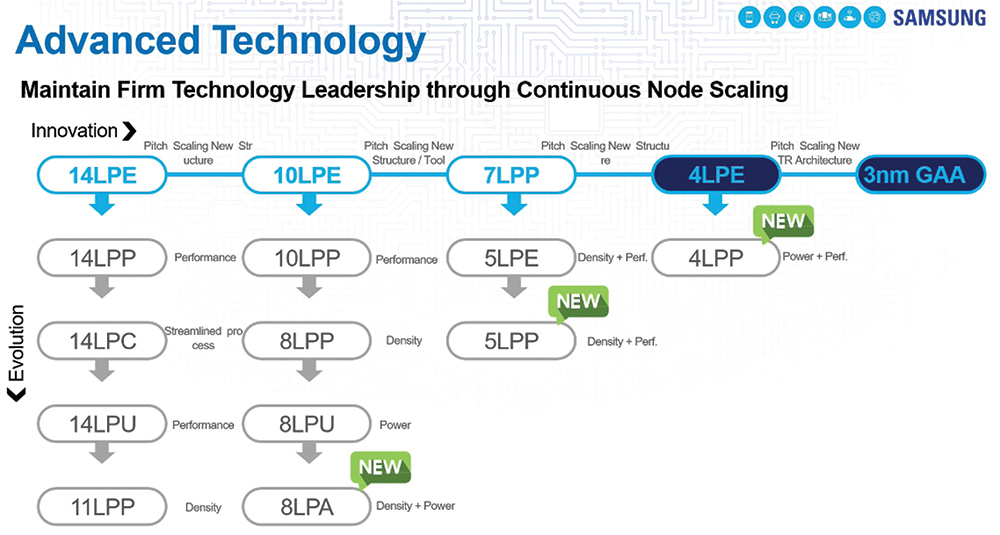
At the annual Samsung Investment Forum 2020 held in late November, Samsung’s foundry service announced that it will build its own 4nm and 3nm chip design ecosystem around Multi-Bridge Channel Field Effect Transistor (MBCFET) and Gate-All-Around Field Effect Transistor (GAAFET) channeling technology.
MBCFET is a new breed of gate channeling technology spun out of the GAA FinFET technology. Comprised of multi-stacked nano sheets, the MBCFET is the more powerful version of GAAFET that does not require additional areas to improve performance. This is because nano sheets can be vertically stacked, while FinFET needs fins to be added laterally.
Logic of 3D FinFET Design
True enough, FinFET 3D transistor structure came on the scene to overcome limitations in voltage scaling of planar transistors – a technology that not only cuts back power consumption, but also improves speed. The typical FinFET transistor is a multi-gate structure where gates are stacked on two, three, or four sides of the channel as if they were built around the channel between the source and drain.
So, the 3D FinFET structure is called gate-all-around, as the channel needs to be fully surrounded by the gate for ideal electronic static. The FinFET structure allows chip makers to further scale down the voltage.
As it is built with nano wires, however, the typical GAA is a very complicated structure to integrate gates, thus compromising technology benefits.
Compatibility with FinFETs
This is the issue that MBCFET structure attempts to deal with. The MBCFETs are compatible with FinFET designs. Hence, chip designers can replace FinFETs with MBCFETs without changing the footprint. Hence, it can be used with power-thrift and high-performance applications, like autonomous driving, artificial intelligence (AI), fifth-generation (5G) mobile communication system, and high-performance computing.
To Release 4nm, 3nm Chip Designs
Samsung foundry plans to release MBCFET-based 4nm Low-Power Early (LPE) and Low-Power Plus (LPP) chips for mobile applications in 2021, while the 3nm MBCFET will roll off the line in 2022.
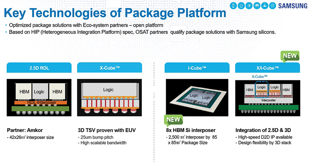
Moreover, Samsung is now working with a new generation of 2.5D and 3D chip packaging technologies called as I-Cube and X/I-Cube. To be commercially available by the end of 2021, these new chip packaging technologies are advanced additions to its predecessor 2.5D RDL and X Cube, both of which are already in volume production stages.
The 2.5D RDL is a low-cost and high-bandwidth solution that is built with 42×26mm2 interposers. I-Cube is a very high-bandwidth solution that enables short memory access latency 3D through silicon via-based small form factor.
A short for interposer-cube, the I-Cube packaging technology is a 2.5D chip packaging solution that connects a logic chip with high bandwidth memory using 2,500mm2 8× High-Bandwidth Memory (HBM) silicon (Si) interposers. The X/I Cube is an integration of X-Cube and I-Cube aimed at providing short memory access latency and high DRAM bandwidth.
Mass production of I-Cube and X/I Cube is scheduled to begin end of 2021.
- Share: