ASIA ELECTRONICS INDUSTRYYOUR WINDOW TO SMART MANUFACTURING
Intel Roadmap Advances Process, Packaging Innovations
Intel Corporation has announced a detailed process and packaging technology roadmaps, showcasing a series of foundational innovations that will power products through 2025 and beyond. In addition to announcing RibbonFET technology, its first new transistor architecture in more than a decade, and PowerVia, a new backside power delivery method, Intel also highlighted its planned swift adoption of next-generation extreme ultraviolet lithography (EUV), referred to as High Numerical Aperture (High NA) EUV. Intel is positioned to receive the first High NA EUV production tool in the industry.

“Building on Intel’s unquestioned leadership in advanced packaging, we are accelerating our innovation roadmap to ensure we are on a clear path to process performance leadership by 2025,” Intel Chief Executive Officer Pat Gelsinger said during the global “Intel Accelerated” webcast. “We are leveraging our unparalleled pipeline of innovation to deliver technology advances from the transistor up to the system level. Until the periodic table is exhausted, we will be relentless in our pursuit of Moore’s Law and our path to innovate with the magic of silicon.”
The industry has long recognized that traditional nanometer-based process node naming stopped matching the actual gate-length metric in 1997. Today, Intel introduced a new naming structure for its process nodes, creating a clear and consistent framework to give customers a more accurate view of process nodes across the industry. This clarity is more important than ever with the launch of Intel Foundry Services. “The innovations unveiled today will not only enable Intel’s product roadmap; they will also be critical for our foundry customers,” Gelsinger said. “The interest in IFS has been strong and I’m thrilled that today we announced our first two major customers. IFS is off to the races!”
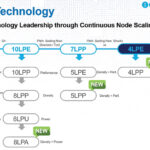
Development Nodes
Intel technologists described the following roadmap with the new node names and the innovations enabling each node:
- Intel 7 delivers an approximately 10 to 15 percent performance-per-watt increase versus Intel 10nm SuperFin, based on FinFET transistor optimizations. Intel 7 will be featured in products such as Alder Lake for client in 2021 and Sapphire Rapids for the data center, which is expected to be in production in the first quarter of 2022.
- Intel 4 fully embraces EUV lithography to print incredibly small features using ultra-short wavelength light. With an approximately 20 percent performance-per-watt increase, along with area improvements, Intel 4 will be ready for production in the second half of 2022 for products shipping in 2023, including Meteor Lake for client and Granite Rapids for the data center.
- Intel 3 leverages further FinFET optimizations and increased EUV to deliver an approximately 18 percent performance-per-watt increase over Intel 4, along with additional area improvements. Intel 3 will be ready to begin manufacturing products in the second half of 2023.
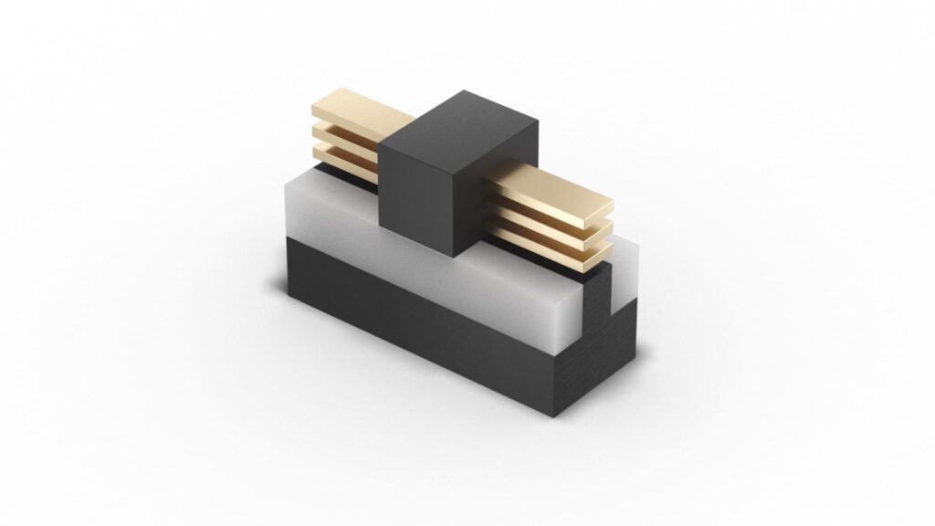
- Intel 20A ushers in the angstrom era with two breakthrough technologies, RibbonFET and PowerVia. RibbonFET, Intel’s implementation of a gate-all-around transistor, will be the company’s first new transistor architecture since it pioneered FinFET in 2011. The technology delivers faster transistor switching speeds while achieving the same drive current as multiple fins in a smaller footprint. PowerVia is Intel’s unique industry-first implementation of backside power delivery, optimizing signal transmission by eliminating the need for power routing on the front side of the wafer. Intel 20A is expected to ramp in 2024. The company is also excited about the opportunity to partner with Qualcomm Incorporated using its Intel 20A process technology.
- 2025 and Beyond: Beyond Intel 20A, Intel 18A is already in development for early 2025 with refinements to RibbonFET that will deliver another major jump in transistor performance. Intel is also working to define, build and deploy next-generation High NA EUV, and expects to receive the first production tool in the industry. Intel is partnering closely with ASML to assure the success of this industry breakthrough beyond the current generation of EUV.
“Intel has a long history of foundational process innovations that have propelled the industry forward by leaps and bounds,” said Dr. Ann Kelleher, Senior Vice President and General Manager of Technology Development. “We led the transition to strained silicon at 90nm, to high-k metal gates at 45nm and to FinFET at 22nm. Intel 20A will be another watershed moment in process technology with two groundbreaking innovations: RibbonFET and PowerVia.”
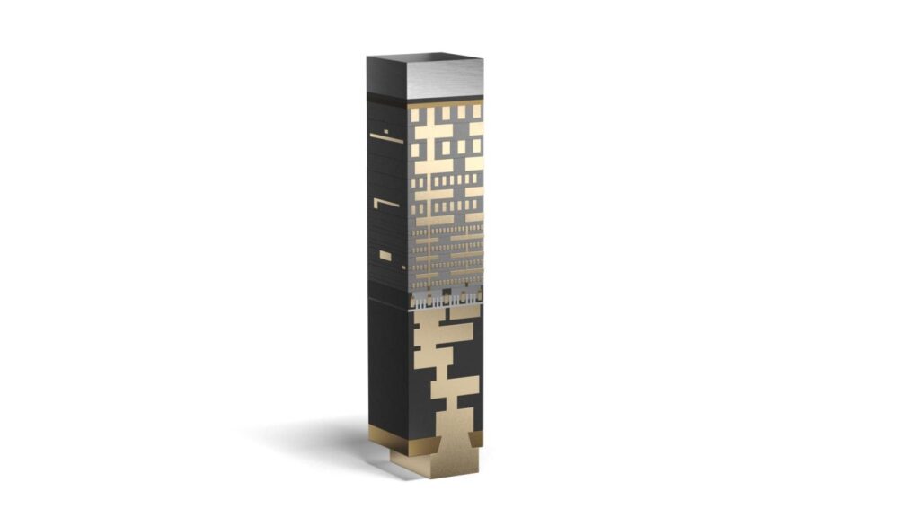
Advanced Packaging Roadmap
With Intel’s new IDM 2.0 strategy, packaging is becoming even more important to realizing the benefits of Moore’s Law. Intel announced that Amazon Web Services will be the first customer to use IFS packaging solutions, while also providing the following insights into the company’s industry-leading advanced packaging roadmap:
- EMIB continues to lead the industry as the first 2.5D embedded bridge solution, with products shipping since 2017. Sapphire Rapids will be the first Intel Xeon data center product to ship in volume with EMIB (embedded multi-die interconnect bridge). It will also be the first dual-reticle-sized device in the industry, delivering nearly the same performance as a monolithic design. Beyond Sapphire Rapids, the next generation of EMIB will move from a 55-micron bump pitch to 45 microns.
- Foveros leverages wafer-level packaging capabilities to provide a first-of-its-kind 3D stacking solution. Meteor Lake will be the second-generation implementation of Foveros in a client product and features a bump pitch of 36 microns, tiles spanning multiple technology nodes and a thermal design power range from 5 to 125W.
- Foveros Omni ushers in the next generation of Foveros technology by providing unbounded flexibility with performance 3D stacking technology for die-to-die interconnect and modular designs. Foveros Omni allows die disaggregation, mixing multiple top die tiles with multiple base tiles across mixed fab nodes and is expected to be ready for volume manufacturing in 2023.
- Foveros Direct moves to direct copper-to-copper bonding for low-resistance interconnects and blurs the boundary between where the wafer ends and where the package begins. Foveros Direct enables sub-10-micron bump pitches, providing an order of magnitude increase in the interconnect density for 3D stacking, opening new concepts for functional die partitioning that were previously unachievable. Foveros Direct is complementary to Foveros Omni and is also expected to be ready in 2023.
The breakthroughs discussed today were primarily developed at Intel’s facilities in Oregon and Arizona, cementing the company’s role as the only leading-edge player with both research and development and manufacturing in the U.S. Additionally, the innovations draw on close collaboration with an ecosystem of partners in both the U.S. and Europe. Deep partnerships are key to bringing foundational innovations from the lab to high-volume manufacturing, and Intel is committed to partnering with governments to strengthen supply chains and drive economic and national security.
- Share: