ASIA ELECTRONICS INDUSTRYYOUR WINDOW TO SMART MANUFACTURING
New Process Innovates Mini, Micro LED Production
Recently, micro light-emitting diodes (microLEDs) have been attracting attention as post thin-film-transistor LCDs (TFT-LCDs) and organic light-emitting diodes (OLEDs). These technological breakthroughs have been among the sought after topics at the recent 21st Photonix (Int’l Laser & Photonics Expo) held last month in Makuhari Messe in Japan’s Chiba prefecture.
This article introduces laser system of Taiwan’s Bolite Co., Ltd. as microLED’s manufacturing technologies and system. The author obtained materials in the booth of Optopia Co., Ltd., a distributor of Bolite.
Company Overview, Original Technologies
Taiwan-headquartered Bolite’s core values are agility, flexibility, and innovation. The company has advanced its laser solutions very uniquely because a very talented team has accumulated extensive know-how over the past 10 years. As a result, the company has developed a laser solution that can strictly control micro scale thermal behavior of laser-materials interactions achieved both in the time and space domains, while integrating lasers of multiple wavelengths (Fig. 1).
Moreover, one of the significant advantages of a laser system with multiple wavelengths is selective processing of heterogeneous structures. As such, stacking up different layers. For example, it can drill vias in one layer without thermally damaging an underlying layer of another material. It also achieves ultrafine feature sizes and high-level precision positioning.
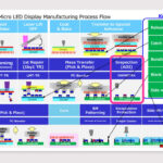
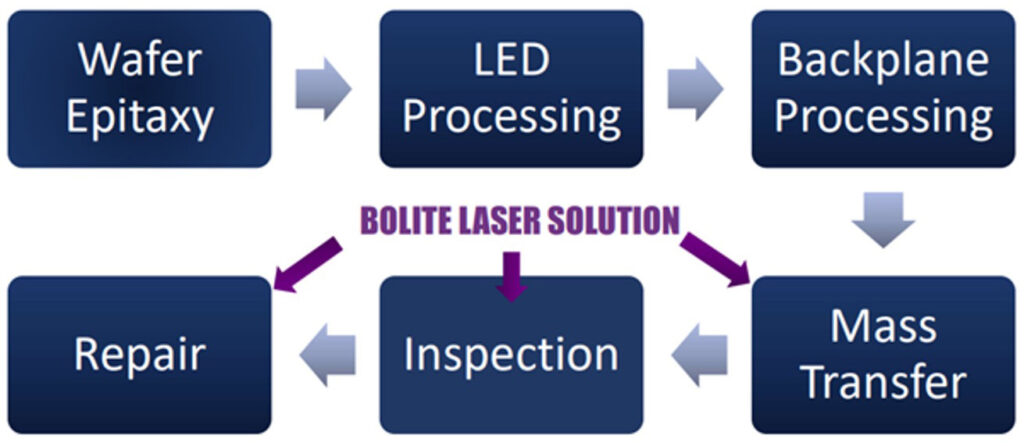
Main Technologies, Challenges of MiniLEDs/MicroLEDs
Fig. 2 shows main technologies of miniLEDs/microLEDs, and Bolite’s laser technology solution. It supports repair, inspection, and mass transfer processes. One of biggest challenges in the manufacturing of microLEDs is how to address the mass transfer process. In the case of 4K displays, even the fastest pick-and-place tool of today takes several weeks to transfer tens of millions of pixels onto the backplane. Meanwhile, effects of the solution to yield are not taken into consideration as placement accuracy of a few microns is required.
Bolite’s MicroLED Manufacturing Technology
Bolite‘s microLED manufacturing process applies laser technology. Firstly, there is the selective laser lift-off (LLO) process. In addition, in microLED display manufacturing, microLEDs are fabricated on gallium nitride (GaN) films grown on sapphire wafers.
Next, GaN-based microLED chips bond onto a temporary carrier. Here, the LLO process separates the sapphire substrate and the GaN intermediate layer via the LLO process.
While this is a reasonably well-established laser process, Bolite provides the added advantage of precise, individual LED selectivity by integrating beam shaping, coaxial imaging, and galvanometer scanning.
Generally, pitches of microLEDs and the display backplane panel for each RGB pixel greatly differ. Bolite has developed a laser-based pitch re-engineering process based on selective LLO for a sequence of bonding/de-bonding steps.
There are several methods for achieving pitch matching. One of them is through the controlled expansion of the carrier substrate. Another approach is the use of chiplets comprised of RGB LEDs and micro ICs.
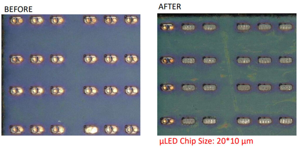
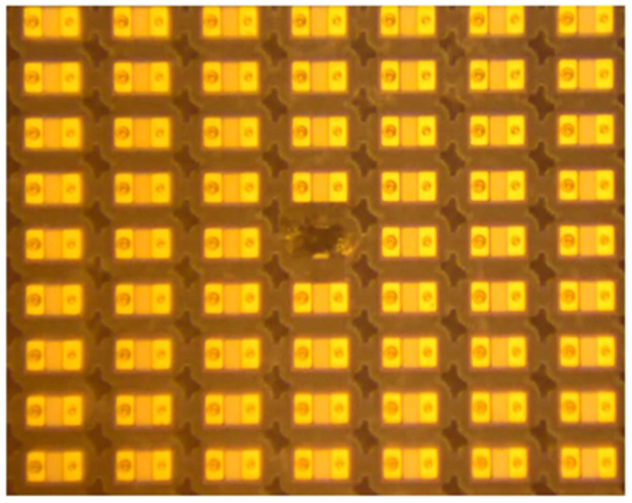
As shown in Fig. 3, Bolite has successfully demonstrated selective LLO of microLEDs as small as 20×10μm from the substrate with high precision. Scanning speed can be as high as 1μs per LED.
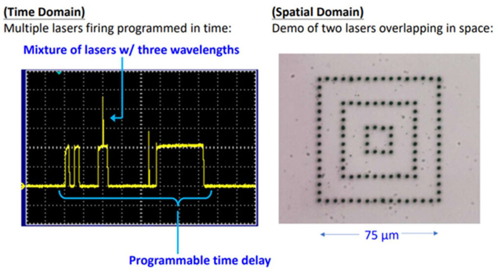
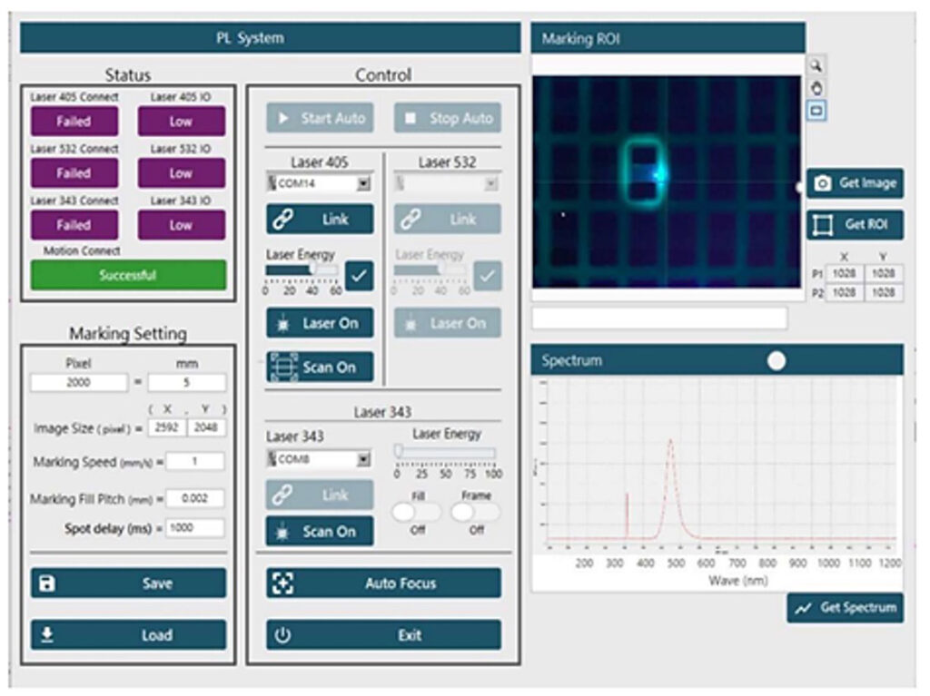
Meanwhile, Bolite is proposing laser-exciting micro photoluminescence (PL) inspection (Fig. 4). Correspondingly, scanning of individual LEDs is possible in this method at a high rate, screened through automated inspection based on their respective PL spectrums.
As a final step to this mass transfer process, Bolite has developed a laser-assisted bonding process for various metals and solders (Fig. 5). This process has stringent requirements regarding process speed, accuracy, and precisely controlled local heating zones confined to minimal areas. Rapid laser heating cycles improves throughput of production, while minimizing the risk of surface oxidation.
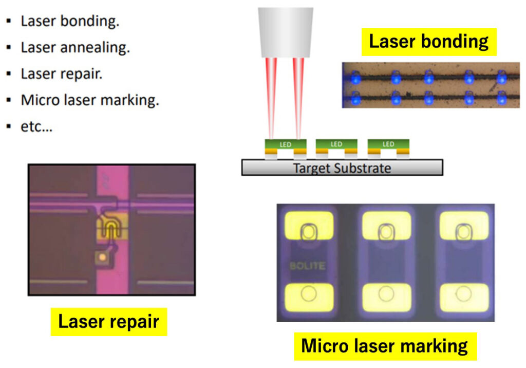
Application of lasers to pattern processing and trimming of defective chips on the substrate (Fig. 6) is also possible. A single defective LED chip can be selectively removed by laser, and then good microLEDs are transferred to complete the repair process.
Bolite is also working on laser marking shown in Fig. 5. The minimum resolution of laser solution to mark batch numbers or production numbers using lasers can be as fine as 1μm. Bolite can also provide development and technical support for barcode and QE-code laser scanning subsystems, as well as complete turnkey solutions.
Advantages of Bolite’s Laser Dicing Solutions
Blade dicing of GaN on silicon (Si) has challenges. These include defects, such as peeling, chipping, and cracks, due to difference in coefficient of thermal expansion (CTE), and the possibility of the peeling of metal if metal film layer exists on the back surface.
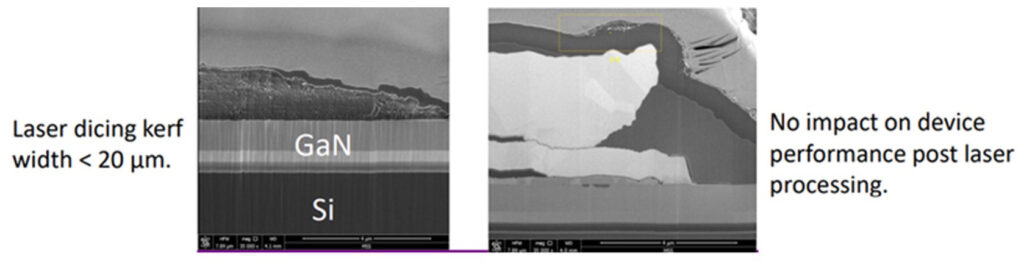
Bolite’s laser dicing solution significantly reduces heat affected zone (HAZ), and hence, reduces defects, and improves yield thanks to cold ablation technology using ultrahigh-speed laser. It also features narrower kerf width. It can reduce the street width to 30μm or smaller from 100μm.
As a result, when creating 1.5mm dies from a 6-inch wafer, the number of chips per wafer increases nearly 10 percent. Fig. 7 shows cross-sectional scanning electron microscopy (SEM) images of laser dicing.
At present, Bolite is working on customized design and growth of III-V semiconductor heterostructures for manufacturing of LEDs and laser diodes, as a development theme. The theme encompasses calculation simulation of quantum well structure, growth of metal oxide chemical vapor deposition (MOCVD) for customized layered heterostructures for LEDs and laser diodes, and development and test of emitters, detectors, and optical subsystems.
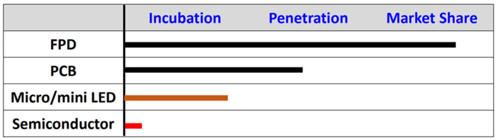
Fig. 8 shows Bolite’s present positions in various industries. MicroLEDs are now in the incubation stage.
- Share:


About This Article:
The author, Yasuhiro Ukai, Ph.D., is from Ukai Display Device Institute (UDDI).