ASIA ELECTRONICS INDUSTRYYOUR WINDOW TO SMART MANUFACTURING
New Technology Takes Chip Bonding to Next Level
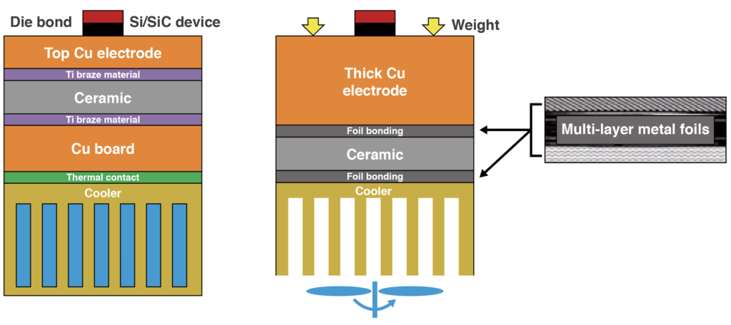
Handotai Netsu Kenkyusho has developed a new technology for mechanically bonding multi-layer metal foils with a low load without heating. Specifically, the technology suits bonding in ceramic insulating substrates with electrodes for silicon (Si) or silicon carbide (SiC) power semiconductor chips. In addition, it also complements bonding between a ceramic insulating substrate with electrodes and a heat-dissipating cooler.
Various metal foils such as aluminum, silver, copper, and tin can employ this new bonding technology. Applying a low load of 3 to 20kgs on several layers of the same or different metal foils realize bonding. Hence, the resulting bond has high thermal conductivity. They are excellent in bonding property, heat resistance, adhesion, flexibility, and elasticity. It can achieve thermal conductivity of 100 W/(m·K) or higher for any multi-layer metal foils.
Reliability, Durability Features
Insulated-gate bipolar transistor (IGBT) chips of Si and SiC mounted on a copper (Cu) electrode, a ceramic insulating substrate, and a cooler. Multi-layer aluminum and silver foils bond together these elements using the new bonding technology. As a result, obtaining thermal conductivity much higher than 100 W/(m·K).
By using metal foils, the bonding part has heat resistance (melting point, etc.), thermal conductivity, and linear expansion coefficient. Hence, comparable to those of general metals. Furthermore, it could relax thermal stress and restore the contact point in the heat stress test. Even if the surface of the metal foils exhibits signs of rusting, they are free from severe oxidation causing thermal insulation.
The single-sided cooling method with a direct bonding copper (DBC) structure suits for mounting Si and SiC power semiconductor chips. The method physically bonds the Cu plate of the upper electrode and the ceramic insulating substrate using silver (Ag) braze containing titanium (Ti). Moreover, bonded the same way are the ceramic insulating substrate and the balance Cu plate for warp countermeasures. Due to physical bonding, however, several issues may occur. These include breaking of ceramic, bonding separation, and die-bond separation due to formation of wavy patterns on the surface of the electrode material. These issues are especially true in a high-temperature heat stress test at 175˚or higher.
Addresses Issues of Conventional Methods
Double-sided cooling type power semiconductor chips are now in practical use. In this case, chemical bonding for upper electrode, thermal contact, ceramic insulating substrate, thermal contact, and a thermal contact with a cooler are possible. This bonding method is flexible, has resistance to thermal stress, and is inexpensive.
However, heat resistance and thermal conductivity remain low. Thus, devices made using this method may not clear the high temperature heat stress test at 200˚ or higher, corresponding to the use for SiC power semiconductors.
Accordingly, the new bonding technology will solve the problems present in these conventional methods. As such, cost reduction is also possible because the balance Cu plate, required for the single-sided cooling method with the DBC structure, is not necessary.
- Share: