ASIA ELECTRONICS INDUSTRYYOUR WINDOW TO SMART MANUFACTURING
New Nanosolder Joining Material Works in Low Temperature
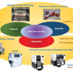
The Manufacturing Innovation Division of Panasonic Holdings Corporation has developed a nanosolder joining material. This innovative joining material enables joining of electronic devices using low-temperature process. After joining, it exhibits heat resistance to 200℃, equivalent to conventional joining materials.
Lean Towards Carbon Neutrality
Growing interests in carbon neutrality are observed in various industries. In the soldering industry, low melting point solders attract attention. Specifically, low melting point solders contribute to power saving of solder baths. Furthermore, they have favorable effects in various processes of soldering, including simplification of the mounting process. As a result, they lead to carbon neutrality.
Elimination of Lead Content
In 1994, Panasonic Holdings started research and development activities to reduce the lead content in joining materials of electronic circuit boards. Meanwhile, in 1998, the company was first to release a product using lead-free solder. Finally, in 2003, it replaced joining materials for all products of the Panasonic Group to lead-free solders.
Further, the company has continued development to increase heat resistance properties of solders; thus, expanding the application range of lead-free solders. The company focused attention on indium (In), which forms a solid solution with tin (Sn), the main component of solder. A solid solution is a solid made by more than two elements melting with each other to have a uniform structure. In 2012, the company commercialized a lead-free solder, which features high heat resistance.
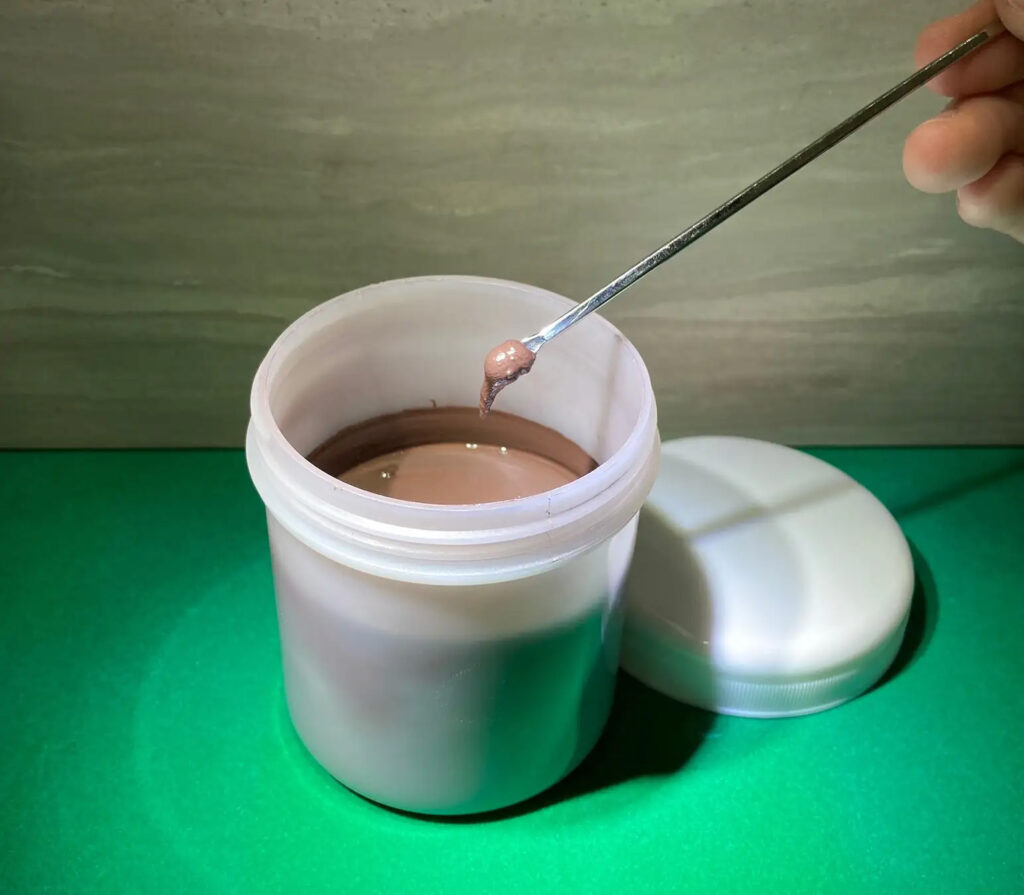
However, the combination of Sn and In has limits in achieving both low-temperature joining and heat resistance property. It was not possible to sufficiently improve heat resistance property, and application areas were limited. Therefore, the company adopted a joining material designed in a way that its solid-liquid reaction proceeds in a short time by controlling the particle diameters of metals. A solid-liquid reaction occurs by combining a low melting point metal and a high melting point metal. This processing method increases reaction speed by melting one material and making it to contact with a solid. As a result, the company has achieved joining at 200℃ by a low-temperature, and short-time process of 10 minutes, and heat resistance to 200℃.
Heat Resistance Approved
Panasonic Holdings has used the developed joining material to produce electronic devices, which successfully cleared the heat resistance test criteria. The company has used ultrasonic cavitation to produce the metal particles, which are materials of the joining material. This method has enabled creation of nanoscale metal particles using less energy than conventional methods. Thus, the developed nanoscale joining material realizes CO2 emissions reduction not only in the manufacturing process of electronic devices, but also in joining material.
For Adoption to Power ICs, Other Devices
Going forward, Panasonic Holdings intends to deploy the joining material to power semiconductor devices and high-frequency devices. The company will leverage the characteristics and superiority of the nanosolder joining material to do this. At the same time, it will accelerate the deployment of the material to a wider range of products by further reducing joining temperature and metal particle size and improving material characteristics. The company promotes its activities toward achieving sustainable society through the reduction of consumption energy.
The nanosolder joining material has achieved joining characteristics comparable to those of conventional silver (Ag) nanopastes. Moreover, it has enabled the achievement of both low-temperature joining in a short time and heat resistance property. Thus, it reduces CO2 emissions, thereby contributing to the protection of global environment.
- Share: