ASIA ELECTRONICS INDUSTRYYOUR WINDOW TO SMART MANUFACTURING
Nikon Releases New Enhanced i-Line Stepper
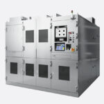
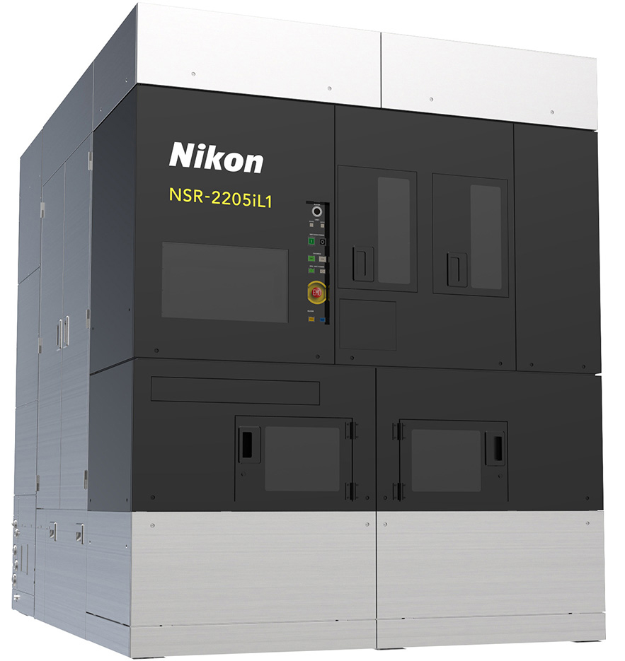
Nikon Corporation announces the release of the NSR-2205iL1 5x reduction i-line stepper. The new lithography system is designed to manufacture a variety of devices such as power and communications semiconductors and MEMS. Also, it is fully compatible with existing Nikon i-line exposure systems.
Specifically, the NSR-2205iL1 provides excellent affordability and enable optimized production of various semiconductor devices regardless of the wafer material. Additionally, it represents the most significant renewal of Nikon 5x stepper technology in the past 25 years. The machine’s system development was in direct response to customer demand for these lithography systems that play such an essential role in chip manufacturing. The new product is set for market release in summer 2024.
Development Background
As electric vehicles, high-speed communications and various IT devices become more prevalent, demand for semiconductors to support them is growing exponentially. These semiconductors must perform a variety of challenging functions. As result, device makers require specialized substrates and exposure systems to manufacture those chips.
Nikon often satisfies these lithography system requirements through means such as refurbishing previously owned steppers. However, refurbished stepper supply can be limited and may not be sufficient to meet customers’ demands. Therefore, to provide additional flexible exposure equipment solutions, Nikon is launching a new 5x i-line stepper that leverages knowledge obtained working closely with customers in order to provide them with specialized solutions. This aims to meet the market’s demand as well as address the limited and aging stepper supply.
In addition to expanding various options to address customers’ diverse needs, this newly developed i-line stepper will also support long-term device production.
Key Benefits
Provides excellent affordability while supporting a variety of needs
Mainly, NSR-2205iL1 will deliver high productivity while optimizing yield level for a variety of semiconductor manufacturing processes through high-accuracy wafer measurement using multipoint autofocus (AF), advanced wafer stage leveling*1, and wide DOF (expanded depth of focus range), among other benefits. In addition, it is well-suited for a variety of applications due to its wafer thickness and size compatibility, high wafer warpage tolerance, and flexible capabilities, including but not limited to, supporting silicon carbide (SiC) and gallium nitride (GaN) processing. The NSR-2205iL1 i-line stepper will deliver excellent affordability while satisfying chipmakers’ diverse requirements.
*1: Mechanism that corrects the shift between the exposure image plane and the substrate surface during exposure. Specifically, it tilts the platform (stage) on which the wafer is placed.
Compatible with existing products and fab operations
Customers having Nikon i-line exposure systems in their fab can continue to utilize assets and operations already in place. Among them include photomasks and wafer exposure recipes. In addition to being compatible with existing fab operations, the 2205iL1 can supplement or replace existing steppers that no longer meet manufacturing requirements.
Designed for long-term use and sustainability
Moreover, NSR-2205iL1 can be used with confidence over an extended period of time because its design utilizes general-purpose commercially available components. This makes it easier than ever to procure parts and provides a more sustainable lithography solution for the future.
