ASIA ELECTRONICS INDUSTRYYOUR WINDOW TO SMART MANUFACTURING
Resonac Eyes New Semiconductor Back End R&D Center
Resonac Corporation has announced plans to establish a research and development center for semiconductor packaging technologies and semiconductor materials in Silicon Valley in the United States. Particularly, Resonac has started to investigate, select, and prepare facilities to be installed in the new R&D center.
The global semiconductor market is likely to exceed US$1 trillion by 2030. Thus, the evolution of AI technologies, including Generative AI, which has been rapidly expanding throughout this year, is accelerating.

Moreover, many cutting-edge semiconductor technologies supporting this trend have originated from Silicon Valley, where many prominent US semiconductor manufacturers, such as Intel and NVIDIA, have bases. Additionally, in recent years, companies such as Google, Apple, Facebook, Amazon, and Microsoft have deployed cloud services including Generative AI services. Most importantly, they also develop their own AI semiconductors.
State-of-the-Art Facilities
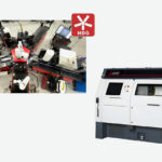
In this context, Resonac has commenced preparations to establish the new Packaging Solution Center (PSC). Particularly, it is a research and development center for advanced semiconductor packaging material technologies, in Silicon Valley, where key figures in development of semiconductor technology concepts gather. The first PSC of Resonac, located in Shin-Kawasaki, Japan, has proven track record. Moreover, it has state-of-the-art facilities that can process large-sized materials such as 300mm wafer and 500mm square panel.
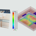
These facilities are capable of laser dicing, fine wiring formation, and handling processes and materials for cutting-edge technologies. Particularly, 2.xD and 3D semiconductor packaging. Thus, the first PSC of Resonac has been serving as a one-stop hub for trial implementation and evaluation of leading-edge production technologies and materials. At the same time, attracting attention of global players in the semiconductor manufacturing industry.
This year, the first PSC has already received visits from more than 150 companies worldwide. To expand such activities, Resonac decided this time to establish the new PSC in the United States. Resonac plans to capture real-time trends and the latest concepts in packaging technology for cutting-edge semiconductors including AI semiconductors. In addition, reflect them in the development of new materials.
Resonac is currently investigating and preparing the equipment to be introduced. Furthermore, it plans to begin operation in 2025 after installing a clean room and equipment.
