ASIA ELECTRONICS INDUSTRYYOUR WINDOW TO SMART MANUFACTURING
New Technology to Pave Way for More Advanced ICs
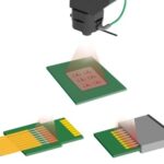
Mitsubishi Electric Corporation, The University of Tokyo, Ajinomoto Fine-Techno Co., Inc. and Spectronix Corporation have developed an ultrafine laser drilling technology necessary for next-generation semiconductor manufacturing. Particularly, the technology can create holes with a diameter of 6μm or smaller in package substrates.
Rising Need for 10μm or Smaller
Until recently, the microfabrication technology in the front-end process to increase integration by making the line width of circuits through exposure on chips have advanced down to 3nm through the advancement of extreme ultraviolet (EUV) lithography technology. However, the microfabrication technology has reached limits in both physical and financial terms.
For that reason, packaging technologies to increase the degree of integration in the back-end process have been attracting attention. These technologies apply three-dimensional (3D) IC packaging technology and a technology called chiplet to integrate chips on packages. 3D chiplet technology wherein SRAMs stacked in vertical direction on CPU dies in package substrates has also been developed.
Thus, drilling process, such as through-silicon vias (TSV), is indispensable in these packaging technologies. Currently, the hole diameter of circuit boards is about 40μm. However, the hole diameter of 10μm or smaller is necessary to manufacture next-generation semiconductors.
Capitalizes Each Strength
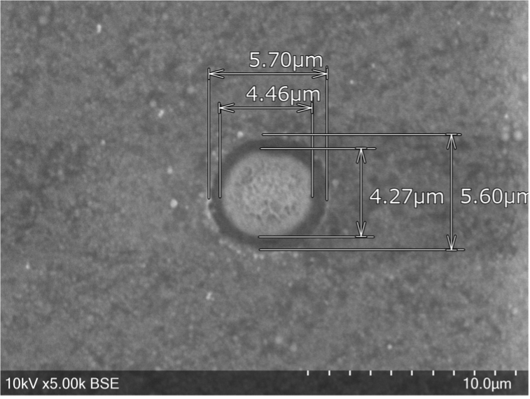
The four corporations that participated in the Consortium for Technological Approaches toward Cool laser Manufacturing with Intelligence (TACMI Consortium) have developed a laser drilling technology. This creates ultrafine holes with a diameter of 6μm.
The TACMI Consortium promotes the co-creation of optical manufacturing under the industry-academia-government cooperation operated by The University of Tokyo.
Furthermore, the four corporations have strengths in different areas relating to the production of semiconductors. They have cooperated across industrial sector boundaries.
In addition, they arranged a 5μm-thick Ajinomoto Build-up Film® (ABF) on a copper thin film and drilled the holes using a laser drilling machine.
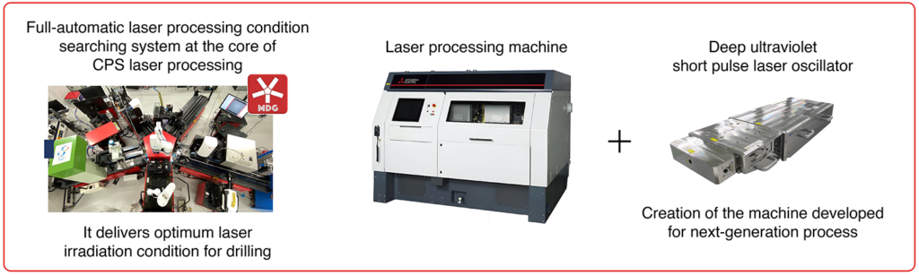
The laser was a deep ultraviolet laser with a 266nm wavelength and a pulse width of picosecond. Spectronix has developed and is marketing the deep ultraviolet laser. The laser processing machine used was Mitsubishi Electric’s machine specially developed for next-generation processes by incorporating a deep ultraviolet short pulse laser.
Meanwhile, The University of Tokyo incorporated the results of the cyber physical system (CPS)-type laser processing machine system, which optimizes the processing process. Moreover, the university is developing the CPS laser processing machine system under the Cross-ministerial Strategic Innovation Promotion Program (SIP). As a result, it has achieved the drilling of ultrafine holes of 6μm or smaller. The technology has achieved drilling capacity of several thousand holes per second.
Meets Future Demands
Furthermore, it has been confirmed that the technology has achieved a taper degree of 75 percent, which is a quality reference value, using parameters for high-definition processing. The taper degree is a ratio of the hole diameter of the upper face and the hole diameter of the lower face of the 6μm diameter.
The ultrafine hole drilling technology is necessary in the back-end process, which supports chiplet technology and multiscale devices in the next-generation semiconductor manufacturing. Hence, this will become increasingly finer and more complex. The use of this will become necessary in the production of advanced semiconductors, for which, the demand for further advancement builds to meet the development of electric vehicles (EVs).
- Share: